Lectures in
Physical Electrons
University of Ninevah
Department of Electronics, Communication and
Computer
in College of Electronic Engineering
by
Dr. Qais Thanon
2017-2018
Chapter 1
Energy bands in Solids
—————————————————————————————————–
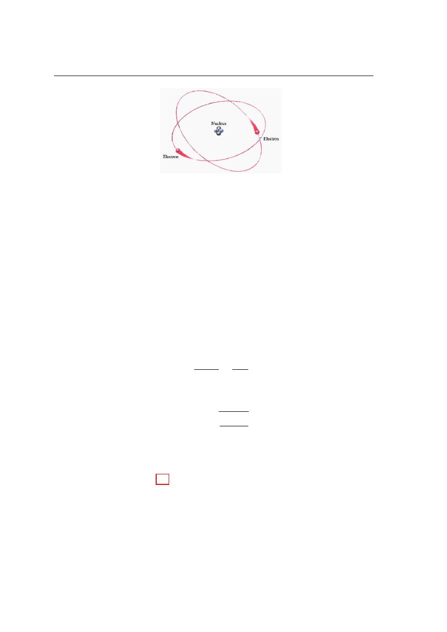
All matters are made of atoms; and all atoms consist of electrons, pro-
tons, and neutrons. In this chapter, you will learn about the structure of
the atom, electron orbits and shells, valence electrons, ions, and the semi-
conductive materials. Semiconductive material is important because the
configuration of certain electrons in an atom is the key factor in determin-
ing how a given material conducts electrical current.
——————————————————————————————————
1.1
Atomic Structure
An atom is the smallest particle of an element that retains the characteristics of that
element. Each atom consists of central nucleus surrounded by orbiting electrons. The
nucleus consists of positively charge particles called protons and uncharged particles
called neutrons. Electrons are the basic particles of negative charge.
CHARGED PARTICLES
Electric charges, positive or negative, occur in multiples of the electronic charge. The
electron is one of the fundamental particles constituting the atom. The charge of an
2
Energy bands in Solids
Figure 1.1: Atomic structure
electron is negative and is denoted by (e). The magnitude of e is 1.6 × 10
−19
Coulomb
and the mass of the electron is 9.1×10
31
kg. The proton have the same charge of electron
but with opposite sign and the mass of proton equal to 1.672 × 10
−27
kg. The charge
of a positive ion is an integral multiple of the charge of the electron, although it is of
opposite sign. For the case of singly ionised particles, the charge is equal to that of the
electron. For the case of doubly ionised particles, the ionic charge is twice that of the
electron.
The electron in obit moving under the influence of the balance between the central
force and the electrostatic force between the electron and the positive nucleus.
e
2
4π
o
r
2
=
mv
2
r
The electron velocity in orbit can be calculated by:
v =
s
e
2
4π
o
mr
(1.1)
Where m is the mass of electron, e is charge of electron and v is electron velocity and
r is the radius of orbit and
o
is the permittivity of space = 8.85 × 10
−12
F/m.
According to equation (1.1) Bohr developed a model which contains three postulates:
1. Instead of infinity of orbits which would be possible in classical mechanics is only
possible for an electron to move in an orbit for which its orbital angular momentum
is an integer multiple by Plank’s constant divided by 2π.
1.1
Atomic Structure
3
P = mvr = n
h
2π
= n~
(1.2)
where
~ =
h
2π
h is Plank’s constant = 6.62 × 10
−34
J s.
Equation (1.2) shows that the angular momentum of electron is quantized. From
equations (1.1) and (1.2) it can be written:
r
n
=
n
2
h
2
o
πme
2
(1.3)
When n=1 equation (1.3) will gives r
1
= 5.29 × 10
−11
m. r
1
≡ Bohr radius ≡
Hydrogen radius (a
o
). Equation (1.3) can be written as:
r
n
= a
o
n
2
(1.4)
where,
a
o
=
h
2
o
πme
2
2. Electromagnetic radiation is emitted if an electron initially moves from an orbit
of total energy (E
i
) to lower orbit of energy (E
f
). The frequency of the emitted
radiation is equal to:
f =
E
i
− E
f
h
(1.5)
3. An atom has a finite state of energy. These states are separated and the electron
in which state is stationary and non-radiating.
4
Energy bands in Solids
1.2
Electron Energy in Orbit
The total energy of electron in orbit around the nucleus is the sum of kinetic energy
and electrostatic energy, that means:
E = electrostatic (work)+ kinetic energy
The potential energy of the electron at a distance r from the nucleus is
−q
2
4π
o
r
, and its
kinetic energy is
mv
2
2
. Then, according to the conservation of energy and using equation
(1.1) we can write:
E =
e
2
8π
o
r
+
−e
2
4π
o
r
(1.6)
The first term in the above equation represents the kinetic energy of the electron
in the orbit whilst the second term represents the work, i.e., the electro-static energy.
The electrostatic energy can be define as the work which required to move an electron
from infinite to distance r from the positive nucleus. As a result the total energy of the
orbital electron can be written as:
E =
−e
2
8π
o
r
(1.7)
It is necessary to observe that equation (1.7) shows that the electron energy is negative
when it bounded to atom. If the total energy of electron is greater than zero,
then the electron has enough energy to separate from atom. Substituting the
value of r from (1.3) in the equation (1.7), the last equation would be as:
E =
−me
4
8h
2
2
o
×
1
n
2
(1.8)
The magnitude
−me
4
8h
2
2
o
is constant and represents the energy of electron in the ground
state of the hydrogen atom. Then it can be re-write equation (1.8) as:
E = E
r
×
1
n
2
(1.9)
1.3
Atomic Energy Level
5
Where E
r
=
−me
4
8h
2
2
o
and the magnitude of this constant is equal to -13.6 eV.
This value is the energy which required to ionize the hydrogen atom.
It can be observed that it is used the electron − volt as a unit of the energy instead
of the ’Joule’. For energies involved in electron devices, ’Joule’ is too large a unit.
Such small energies are conveniently measured in electron − volt, abbreviated eV . The
electron − volt is defined as the kinetic energy gained by an electron, initially at rest,
in moving through a potential difference of 1 volt. Since e = 1.6 × 10
−19
Coulomb, then
each 1eV will equal to 1.6 × 10
−19
Joule.
1eV = 1.6 × 10
−19
Joule.
1.3
Atomic Energy Level
According to equation (1.9) the energy of second state is -3.4ev. Then it is required
to 10.2ev to raise the electron from ground state to second state. Therefore there is
only discrete value of electron energy exist within atomic structures. This energy can
be calculate using the following equation:
∆E = E
R
×
1
n
2
i
−
1
n
2
f
!
(1.10)
For each integral value of n in equation (1.9) a horizontal line is drawn. These lines
are arranged vertically in accordance with the numerical values calculated from equa-
tion (1.9). Such graph is called an energy-level diagram and is indicated in Fig. 1.2 for
hydrogen. The number to the left of each line gives the energy of this level in electron
volts. The number immediately to the right of a line is the value of n. Theoretically,
an infinite number of levels exist for each atom, but only the first five and the level for
n = ∞ are indicated in Fig. 1-2.
As the electron is given more and more energy, it moves into stationary states which
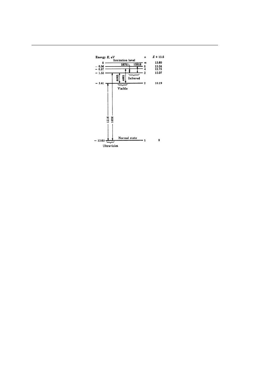
6
Energy bands in Solids
Figure 1.2: The lowest five energy levels and the ionization level of hydrogen. The
spectral lines are in angstrom units.
are farther and farther away from the nucleus. When its energy is large enough to
move it completely out of the field of influence of the ion, it becomes ’detached’ from
it. The energy required for this process to occur is called the ionization potential and is
represented as the highest state in the energy-level diagram.
1.3
Atomic Energy Level
7
Solved problems
1. Calculate the electron velocity in the second orbit of the hydrogen atom?
Solution
According to equation (1.1) the electron velocity in the orbit is given by:
v =
q
e
2
4π
o
mr
Since r = a
o
×n
2
r = 5.29 × 10
−11
× 2
2
= 2.11 × 10
−10
m.
v =
q
(1.6×10
−19
)
2
4π×8.85×10
−12
×9.1×10
−31
×2.11×10
−10
v = 1.96 × 10
6
m.s
−1
.....................................................
2. The total energy of electron in the second orbit is (-3.4ev).
Find the
kinetic energy and work?
Solution
As it is shown before in equation (1.6) that the total energy of the electron in the
orbit is the sum of kinetic energy and work. Then, E=K.E + W
but K.E =
e
2
8π
o
r
and W =
−e
2
4π
o
r
then E =
e
2
8π
o
r
+
−e
2
4π
o
r
=
−e
2
8π
o
r
=-K.E=
W
2
K.E = −E = −(−3.4) = 3.4 eV
W = 2 × E = 2 × −3.4 = −6.8 eV
.....................................................
3. A photon with energy of 5eV is emitted for electron transition from or-
bit to another.
Find the wavelength of the emitted electromagnetic wave?
Solution
E = h × ν =
h×c
λ
λ =
h×c
E
=
6.62×10
−34
×3×10
8
5×1.6×10
−19
=0.24 µ m.
.....................................................
8
Energy bands in Solids
4. What is the frequency of the electromagnetic wave which emitted from
the electron transition from the second orbit to the first orbit?
Solution
∆E = E
R
×
1
n
2
i
−
1
n
2
f
= −13.6 ×
1
2
2
−
1
1
2
= 10.2eV
1.4
De Broglie Hypothesis
Since a photon is absorbed by only one atom, the photon acts as if it were con-
centrated in a very small volume of space, in contradiction to the concept of a wave
associated with radiation. De Broglie postulated that the dual character of wave and
particle is not limited to radiation, but is also exhibited by particles such as electrons,
atoms, or macroscopic masses. He postulated that a particle of momentum p = mv has
a wavelength λ associated with it given by:
λ =
h
P
(1.11)
We can make use of the wave properties of a moving electron to establish Bohr’s postulate
that a stationary state is determined by the condition that the angular momentum
must be an integral multiple of (h/2π). It seems reasonable to assume that an orbit of
radius r will correspond to a stationary state if it contains a standing-wave pattern. In
other words, a stable orbit is one whose circumference is exactly equal to the electronic
wavelength λ, or to (nλ), where n is an integer (but not zero). Thus:
2πr = nλ =
nh
mv
(1.12)
Prove equation 1.12?
1.5
The energy-band theory of crystals
9
1.5
The energy-band theory of crystals
As we have seen, all the electrons of a given atom having the same value of n belong
to the same prescribed bands (electronic shell). Each shell around the nucleus corre-
sponds to a certain energy band and is separated from adjacent shells by energy gaps,
in which no electron can exist.
A crystal is a solid consisting of a regular and repetitive arrangement of atoms or
molecules (strictly speaking, ions) in space. If the positions of the atoms in the crystal
are represented by points, called lattice points, we get a crystal lattice. The distance
between the atoms in a crystal is fixed and is termed the lattice constant of the crystal.
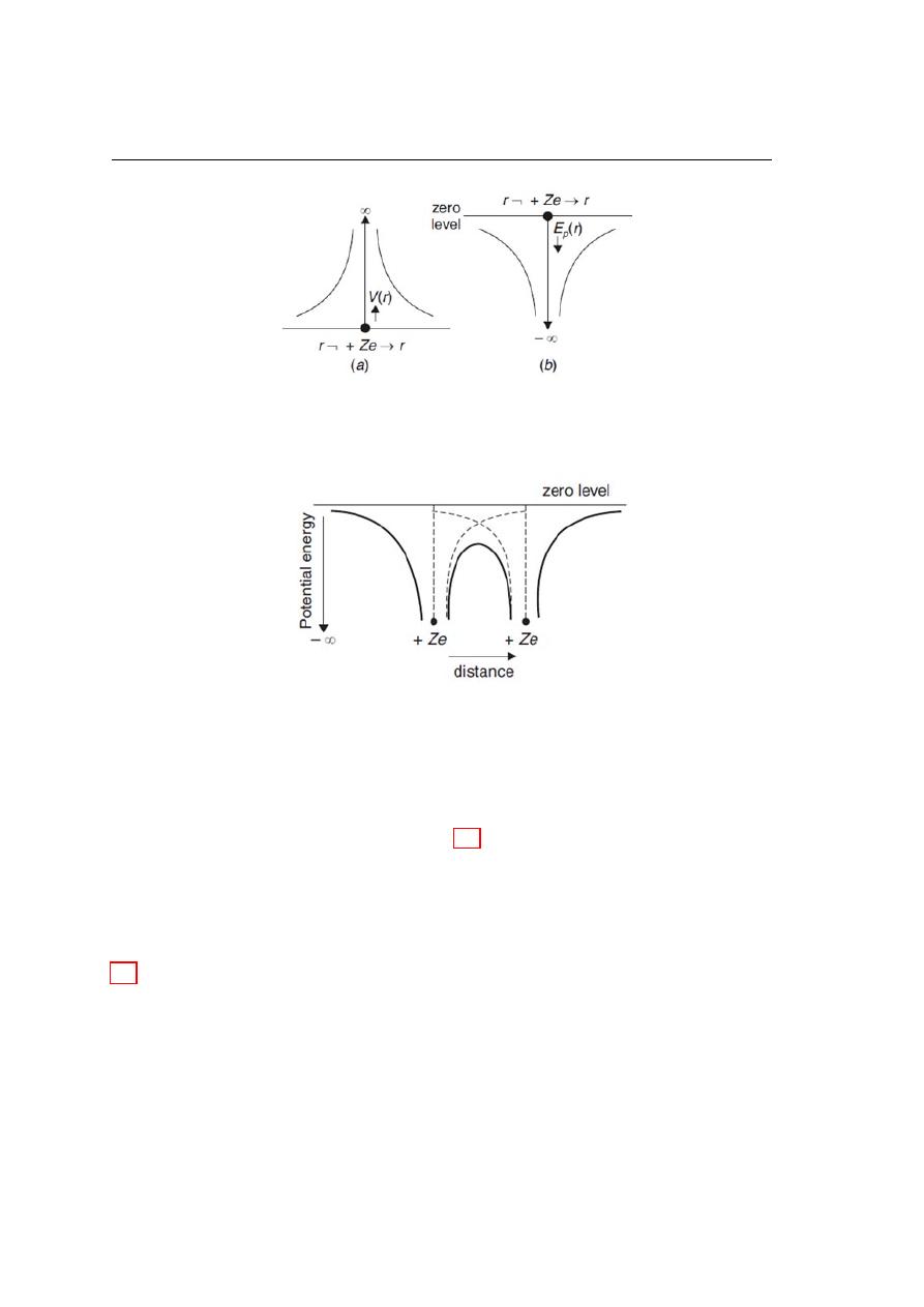
To discuss the behaviour of electrons in a crystal, we consider an isolated atom of the
crystal. If Z is the atomic number, the atomic nucleus has a positive charge Ze. At a
distance r from the nucleus, the electrostatic potential due to the nuclear charge is (in
SI units).
V (r) =
Ze
4π
o
r
(1.13)
Since an electron carries a negative charge, the potential energy of an electron at a
distance r from the nucleus is:
E
p
(r) = −eV =
−Ze
2
4π
o
r
(1.14)
V (r) is positive while E
p
(r) is negative. Both V (r) and E
p
(r) are zero at an infinite
distance from the nucleus. Figs. 1.3(a) and (b) show the variation of V (r) and E
p
(r),
respectively with r.
Now, consider two identical atoms placed close together. The net potential energy of
an electron is obtained as the sum of the potential energies due to the two individual
nuclei. In the region between the two nuclei, the net potential energy is clearly smaller
than the potential energy for an isolated nucleus (see Fig. 1.3).
10
Energy bands in Solids
Figure 1.3: Variation of (a) Potential in the field of a nucleus with distance, (b) Potential
energy of an electron with its distance from the nucleus.
Figure 1.4: Potential energy variation of an electron with distance between two identical
nuclei.
The potential energy along a line through a row of equispaced atomic nuclei, as in a
crystal, is diagrammatically shown in figure 1.5. The potential energy between the nuclei
is found to consist of a series of humps. The separation between the split-off energy levels
is very small. This large number of discrete and closely spaced energy levels forms an
energy band. Energy bands are represented schematically by shaded regions in figure
1.5(b).
The width of an energy band is determined by the parent energy level of the isolated atom
and the atomic spacing in the crystal. The lower energy levels are not greatly affected
by the interaction among the neighbouring atoms, and hence form narrow bands. The
higher energy levels are greatly affected by the interatomic interactions and produce
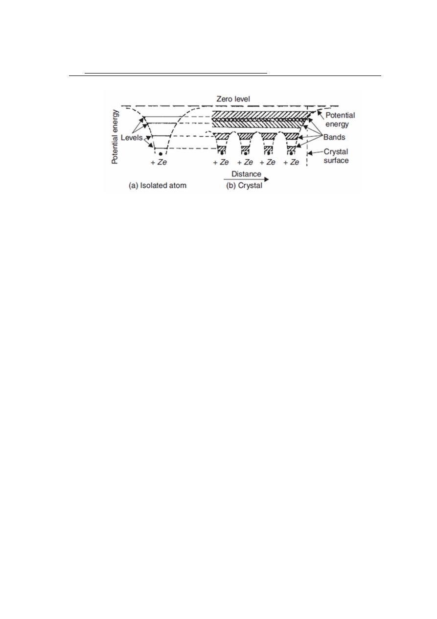
1.5
The energy-band theory of crystals
11
Figure 1.5: Splitting of energy levels of isolated atoms into energy bands as these atoms
are brought close together to produce a crystal.
wide bands.
The lower energy bands are normally completely filled by the electrons since the electrons
always tend to occupy the lowest available energy states. The higher energy bands may
be completely empty or may be partly filled by the electrons.
The interatomic spacing, although fixed for a given crystal, is different for different
crystals. The width of an energy band thus depends on the type of the crystal, and is
larger for a crystal with a small interatomic spacing. The lower energy bands are
normally completely filled by the electrons since the electrons always tend to
occupy the lowest available energy states. The higher energy bands may be
completely empty or may be partly filled by the electrons. The lower energy
band calls the valence band and the first, unfilled or partially filled, band above the
valence is called conduction band. The energy gap between the valence and conduction
can be calculated as:
E
g
= E
c
− E
v
(1.15)
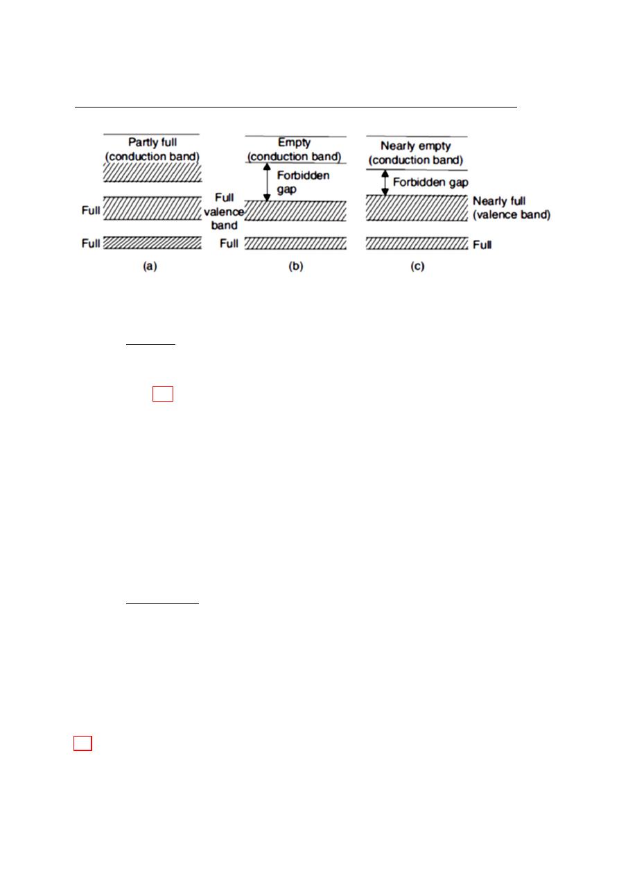
On the basis of the band structure, crystals can be classified into metals, insulators,
and semiconductors.
12
Energy bands in Solids
Figure 1.6: Energy band structure of (a) metal, (b) insulator, and (c) semiconductor.
1.5.1
Metals
A crystalline solid is called a metal if the uppermost energy band is partly
filled [figure 1.6(a)] or the uppermost filled band and the next unoccupied
band overlap in energy. The electrons in the uppermost band find neighbouring va-
cant states to move in, and thus behave as free particles. In the presence of an applied
electric field, these electrons gain energy from the field and produce an electric current,
so that a metal is a good conductor of electricity. The partly filled band is called the
conduction band. The electrons in the conduction band are known as free electrons or
conduction electrons.
1.5.2
Insulators
When the forbidden energy gap between the valence band and the conduction band,
is very large, only a few electrons can acquire enough thermal energy to move from the
valence band into the conduction band. Such solids are known as insulators. Since only
a few free electrons are available in the conduction band, an insulator is a bad conductor
of electricity. The energy band structure of an insulator is schematically shown in figure
1.6(b).
1.6
Fermi−Dirac distribution function
13
1.5.3
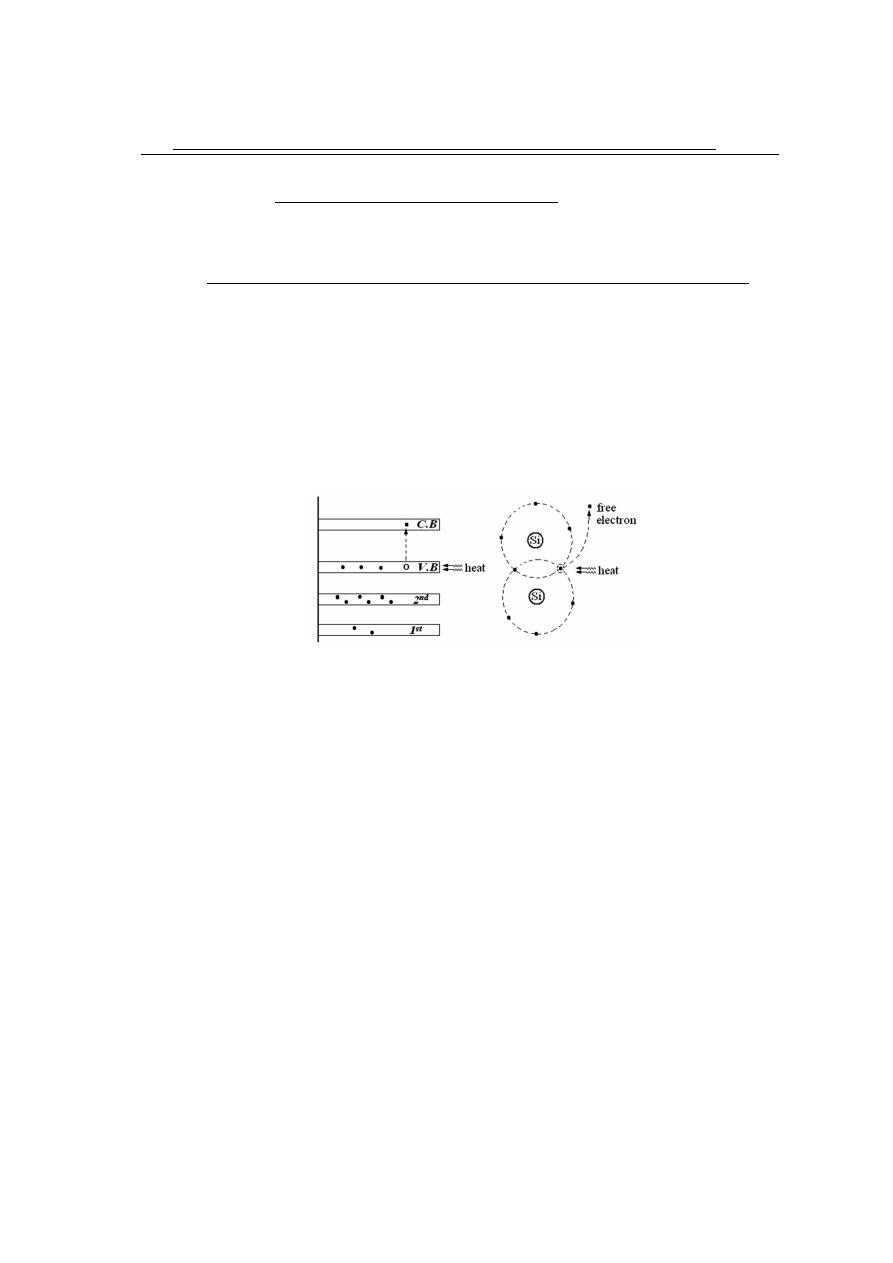
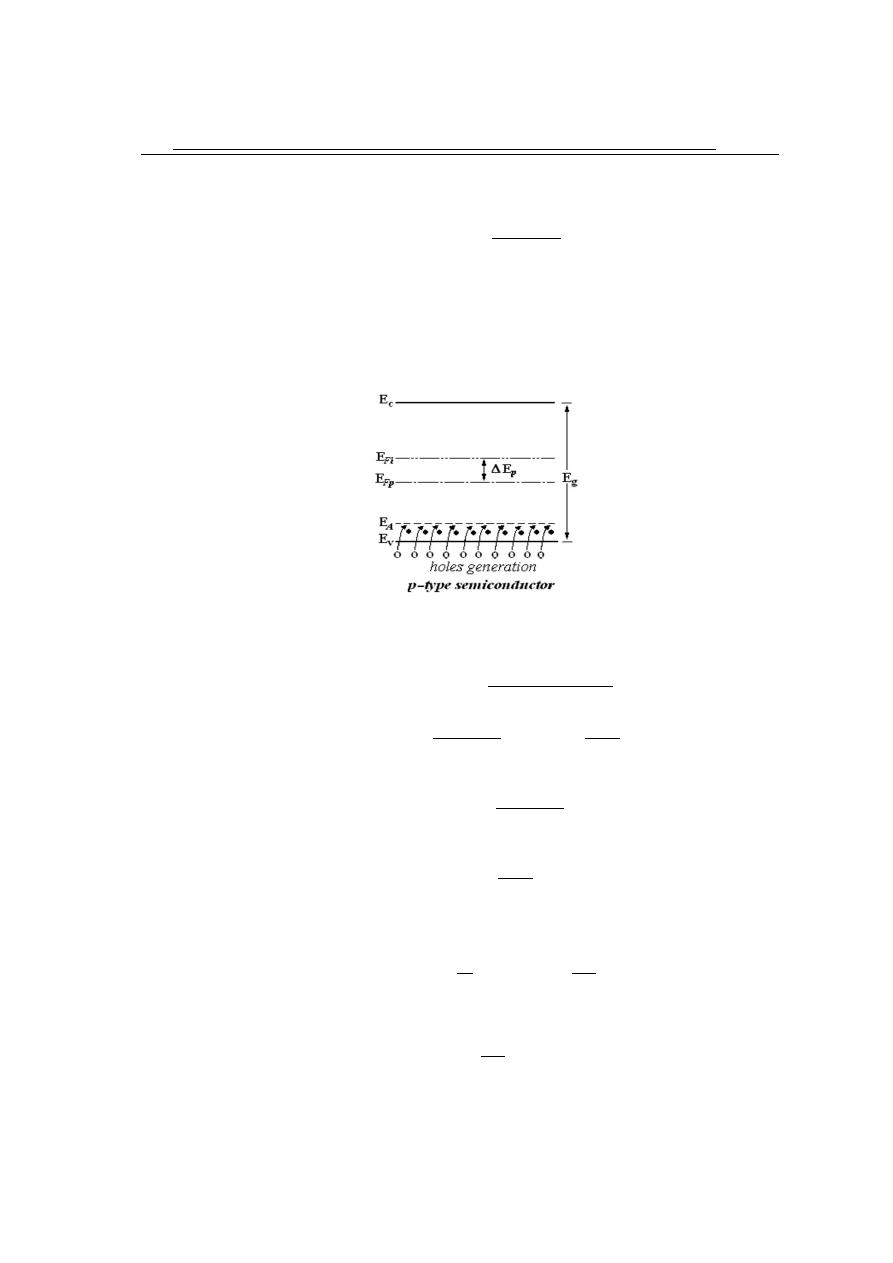
Semiconductors
A material for which the width of the forbidden energy gap between the valence and
the conduction band is relatively small ( 1 eV) is referred to as a semiconductor. As the
forbidden gap is not very wide, some of the valence electrons acquire enough thermal
energy to go into the conduction band. These electrons then become free and can move
about under the action of an applied electric field. The absence of an electron in the
valence band is referred to as a hole. The holes also serve as carriers of electricity. The
electrical conductivity of a semiconductor is less than that of a metal but greater than
that of an insulator. The band diagram of a semiconductor is given in figure 1.6(c).
At 0
o
K the semiconductor becomes insulator because the electrons do not has energy
to jump to conduction band.
1.6
Fermi−Dirac distribution function
Fermi Dirac distribution function describes the energies of single particles in a system
comprising many identical particles that obey the Pauli exclusion principle. Electrons
are Fermions, and thus follow Fermi Dirac distribution function.
At room temperature, the thermal energy of the atoms may allow a small number of
electrons to participate in the conduction process in semiconductor. The probability for
filling the band by electrons depends on temperature.
f (E) =
1
1 + exp
E−E
f
kT
(1.16)
where f (E) is the probability of occupancy of the state with energy E, E
F
is a char-
14
Energy bands in Solids
acteristic energy for a particular solid and is referred to as the Fermi level, T is the
absolute temperature in
o
K and k is Boltzmann’s constant (k = 1.38 ×10
−23
J K
−1
=
8.614 ×10
−5
eV K
−1
). Fermi energy can be defined as the energy at which there would
be a fifty percent chance of finding an electron.
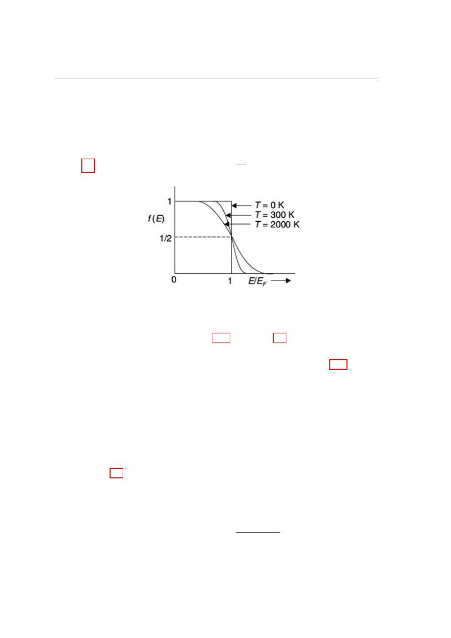
Figure 1.7 shows the probability f (E) against
E
E
F
for T = 0, 300 and 2000 K.
Figure 1.7: f (E) as a function of E/E
F
for different values of T
From Fermi Dirac function, equation 1.16 and figure 1.7, it can be conclude that:
1. At the absolute zero of temperature, i.e. at T = 0 K, equation 1.16 shows that
f (E) = 1 for E < E
F
and f (E) = 0 for E > E
F
. Thus all the energy states
below E
F
are occupied by the electrons and all the energy states above E
F
are
completely empty. (The probability of finding electron above Fermi level at zero
o
K is zero).
2. At temperatures greater than the absolute zero, f (E) > 0 for E > E
F
, as shown
in figure 1.7. This means that at a finite temperature, some of the electrons in the
quantum states below EF acquire thermal energy to move into states above E
F
.
The probability of electron above Fermi level at T >0
o
K is given by:
f (E) = exp
− (E − E
f
)
kT
(1.17)
1.6
Fermi−Dirac distribution function
15
3. The probability of electron to fill a state below Fermi level at T >0
o
K is given by:
f (E) = 1 − exp
− (|E − E
f
|)
kT
(1.18)
Solved problems
1. Find the probability of an electron to occupy a level (0.1 eV) above
Fermi level at 27
o
C?
Solution
f (E) = exp
−
(
E−E
f
)
kT
= exp
−(0.1)
8.614×10
−5
×300
= 0.0209
2. The probability for an electron to occupy a level at 120
o
C is (2×10
−6
).
Find the location of this level with respect to Fermi level?
Solution
f (E) =
1
1+exp
E−Ef
kT
=
1
1+exp
E−Ef
8.614×10−5×300
= 2 × 10
−6
E − E
f
= 0.444eV above Fermi level.
Review Questions
1.
What is the orbital angular momentum of the electron in the third orbit? (Ans. 3×~ =
1.97 × 10
−15
eV ).
2. What is the energy of the electron in the Hydrogen atom after absorption an electro-
magnetic wave with frequency of 3.284 × 10
15
Hz?(Ans. 13.59 eV).
3. An electron, initially at rest, gains a speed of 10
7
m/s after being accelerated through
a potential difference of V volt. Determine V. What is the final kinetic energy of the
electron in J and eV? (Ans. 284.7 volt, 4.555 × 10
−17
J , 284.7 eV)

16
Energy bands in Solids
4. A particle carries a positive charge numerically equal to the electronic charge. It acquires
a velocity of 200 km/s after moving through a potential difference of 210 V. Determine
the mass of the particle relative to the electronic rest mass. (Ans. 1844 m
o
).
5. A particle of charge 1.2 × 10
−8
C and mass 5g travels a distance of 3m under the action
of a potential difference of 500V . Calculate the final velocity and the acceleration of the
particle if it starts from rest. (Ans. 4.898 × 10
−2
m/s, 4 × 10
−4
m/s
2
).
6. A potential difference of 400 volt is applied between two parallel metal plates 4 cm apart.
An electron starts from rest from the negative plate. Obtain (i) the kinetic energy of
the electron when it reaches the positive plate and (ii) the time required by the electron
to reach the positive plate. (Ans. 400 eV, 6.745 × 10
−9
s).
7. Find the probability for an electron to occupy a level at 50
o
C if this level is below Fermi
level by (0.2 eV)?

Chapter 2
Transport Phenomena in
Semiconductor
—————————————————————————————————–
The current is defined as the flow of charge particles.
In metal the
current results from the flow of negative charges (electrons),whereas the
current in a semiconductor results from the motion of both electrons and
positive charges (holes). A pure semiconductor may be doped with impu-
rity atoms so that the current is due predominantly either to electrons or
to holes. The transport of the charges, i.e. conductivity, in a crystal under
the influence of an electric field (a drift current), and also as a result of a
nonuniform concentration gradient (a diffusion current), is investigated in
this chapter.
——————————————————————————————————
2.1
Mobility and Conductivity
As it is observed in the preceding chapter, according to the energy band theory, the
materials can be classified into three types: insulators, conductors and semiconductors.
A conductor is a solid in which an electric current flows under the influence of the electric
field. By contrast, application of an electric filed produces no current in an insulator.
18
Transport Phenomena in Semiconductor
The energy gap for an insulator is so wide that hardly any electrons acquired enough
to jump to conduction band. If a constant electric field is applied to the metal, the
electrons will move with acceleration equal:
a =
e E
m
(2.1)
where, E is the electric field in unit (V m
−1
)
But the electron suffering from collisions with other particles in metal and it speed
between two successive collisions is (a t). t : is the relaxation time. The distance between
two successive collisions is called the mean free path and equal to:
l = v
d
t
(2.2)
Electrical mobility is the ability of charged particles (i.e. electrons) to move through
a medium in response to an electric field that is pulling them. The external electrical
field gives electron drift velocity and acceleration, therefore the drift velocity is equal
to:
v
d
= µ E
(2.3)
where µ is the electron mobility in unit (m
2
V
−1
s
−1
) and it is equal to (et/m).
The minus sign means the drift velocity is in the direction opposite to that of the external
electric field.
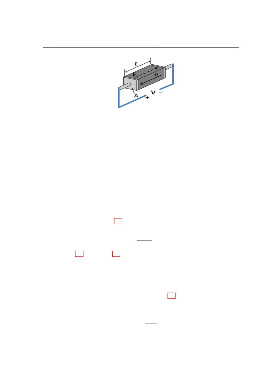
Electrical Conductivity:
Electrical conductivity is a measure of a material’s ability to
conduct an electric current. It is commonly represented by Greek letter σ. The following
figure shows a box of metal with length L and cross section area A. The voltage V was
applied on the ends of the box. According to Ohm’s law: V = I R
and;
R = ρ
L
A
(2.4)
where ρ is the resistivity in unit (Ωm).
Since R = V /I
Then 2.4 becomes:
(I/A) = (1/ρ) × (V /L) = J (Current density)
but (V /L) = E and (1/ρ) = σ, then:
2.1
Mobility and Conductivity
19
Figure 2.1: Box of metal
J = σ E
(2.5)
Where J represents the drift current density.
Now, consider that the metal contains (n) of free electrons per unit volume, then the
total free electrons inside the metal is:
q = −n e A L
(2.6)
but I = (q/t) = q × (v
d
/L), where v
d
= (L/t)
Since I = J × A and from 2.5 we have J = σ E, then it can be write:
σE = −q
v
d
L × A
= −n e v
d
(2.7)
Substituting 2.7 in equation 2.3, we can obtain:
σ = −n e µ
(2.8)
This equation shows that the conductivity depends on the density of the free elec-
trons and the mobility of these electrons. Equation 2.8 can be written in new form as
shown below:
σ =
n e
2
l
m v
d
(2.9)
20
Transport Phenomena in Semiconductor
2.2
Diffusion Current
In addition to a conduction current, the transport of charges in a semiconductor
may be accounted for by a mechanism called diffusion, not ordinarily encountered in
metals. The essential features of diffusion are now discussed.
It is possible to have a
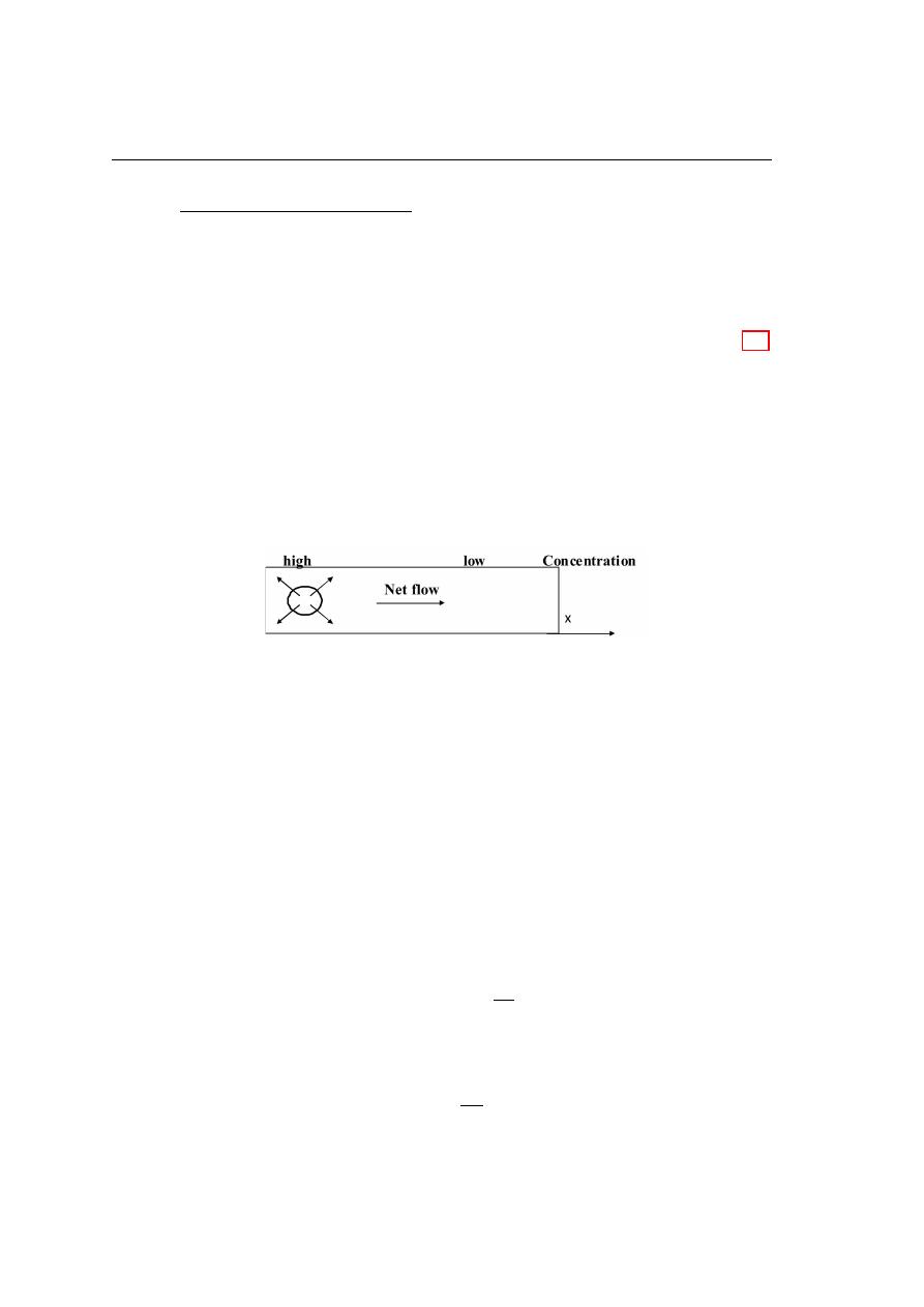
nonuniform concentration of particles in a semiconductor. As indicated in figure 2.2, the
concentration n of electrons varies with distance x in the semiconductor, and there exists
a concentration gradient, dn/dx, in the density of carriers. The existence of a gradient
implies the density of electrons immediately on one side of the surface is larger than
the density on the other side. The electrons are in a random motion as a result of their
thermal energy. Accordingly, electrons will continue to move back. The net transport
of electrons across the surface constitutes a current in the positive X direction.
Figure 2.2: A nonuniform concentration n(x) results in a diffusion current
It should be noted that this net transport of charge is not the result of mutual re-
pulsion among charges of like sign, but is simply the result of a statistical phenomenon.
This diffusion is exactly analogous to th at which occurs in a neutral gas if a concentra-
tion gradient exists in the gaseous container. The diffusion electron-current density J
n
(amperes per square meter) is proportional to the concentration gradient, and is given
by:
J
dif f
∝ (dn/dx)
also,
J
dif f
∝ D
where D is diffusion constant (m
2
sec
−1
)
J
dif f
= e D
dn
dx
(2.10)
D and µ are related by Einstein relation:
D =
kT
e
µ
(2.11)
2.3
Work Function
21
where T is the temperature in
o
K
Total Current: It is possible for both a potential gradient and a concentration gradient
to exist simultaneously within a semiconductor. In such a situation the total hole current
is the sum of the drift current 2.5 and the diffusion current 2.10;
J
tot
= eD
dn
dx
+ σE
(2.12)
2.3
Work Function
Free electron moves in metal by random motion in absent external operator or in
additional to drift and /or diffusion motion. The kinetic energy makes electrons reach
Fermi level. Then the energy required rising electron to state outside the metal is E
s
(surface energy), therefore the work function (φ ) given as:
φ = E
s
− E
f
(2.13)
The work function is the minimum energy (usually measured in electron volts)
needed to remove an electron from a solid to a point immediately outside the solid
surface (or energy needed to move an electron from the Fermi level into vacuum). Here
”immediately” means that the final electron position is far from the surface on the
atomic scale but still close to the solid on the macroscopic scale. The work function
is a characteristic property for any solid phase of a substance with a conduction band
(whether empty or partly filled). For a metal, the Fermi level is inside the conduction
band, indicating that the band is partly filled. For an insulator, the Fermi level lies
within the band gap, indicating an empty conduction band; in this case, the minimum
energy to remove an electron is about the sum of half the band gap and the electron
affinity. When the electron absorbs energy E then the K.E. for this electron outside the
metal will be:
1
2
m v
2
= E − φ
(2.14)
This is called electronic emission.
There is four type of electronic emission:
Thermionic Emission, Photo Emission, Field Emission and Secondary Emission.
If
22
Transport Phenomena in Semiconductor
a thermal energy is supplied to the electrons in the metal, then the energy distribution
of the electrons changes, because of the increasing in the temperature. The thermal
energy given to the charge carrier overcomes the binding potential (work function) and
can release it from the metal surface. This is called Thermionic emission. According
to the Richardson-Dushman equation the emitted electron current density, J (A.m
−2
),
is related to the absolute temperature T by the equation:
J = A
o
T
2
exp(
−φ
kT
)
(2.15)
where (A
o
) is Richardson-Dushman constant. As mentioned before, the work func-
tion is the minimum energy that must be given to an electron to liberate it from the sur-
face of a particular substance. In the photoelectric effect, electron excitation is achieved
by absorption of a photon. If the photon’s energy is greater than the substance’s work
function, photoelectric emission occurs and the electron is liberated from the surface.
Excess photon energy results in a liberated electron with non-zero kinetic energy. The
photo-electric work function is:
φ = hf
o
f
o
is the minimum (threshold) frequency of the photon required to produce photo-
electric emission.
Field emission (F
E
) (also known as field electron emission and electron field
emission) is emission of electrons induced by an electrostatic field. Field emission in
pure metals occurs in high electric fields and strongly dependent upon the work function.
The emission current density is given as:
J ∝ exp (
−φ
e E x
o
)
(2.16)
x
o
is the gap thickness.
Secondary electron emission is a phenomenon where primary incident electrons
of sufficient energy, when hitting a surface of material, induce the emission of secondary
electrons. It was found experimentally the number of secondary electrons depend on
the following the number and the energy of primary electrons, the angle of incidence of
the particles on the material, the type of the material, and the physical condition of the
surface. The secondary emission ratio (δ) defined as:
2.3
Work Function
23
δ =
no. of the secondary emitted electrons
no. of the primary incident electrons
(2.17)
Solved problems
1. A silicon crystal having across section area of (0.001cm
2
) and a length
of (10
−3
cm) is connected at its ends to (10V ) battery at temperature
(300
o
K).
Find the resistivity and the conductivity of the silicon crys-
tal if the current passing through the crystal is (100mA).
Solution
J = σ E ⇒ σ =
J
E
=
I/A
V /L
σ =
100 × 10
−2
/0.001 × 10
−4
10/(10
−3
× 10
−2
)
= 10 (Ωm)
−1
ρ =
1
σ
=
1
10
= 0.1 Ω m
.....................................................
2. Calculate the average drift velocity of hole in a bar of silicon with
across sectional area (10
−4
cm
2
), containing holes concentration of (4.5×
10
15
cm
−3
) and carrying a current of (45mA)?
Solution
v
d
= µ E.....(a)
σ = pe µ.....(b)
J = σE ⇒ σ =
J
E
.....(c)
Therefore equation (b) becomes:
J
E
= peµ ⇒ µ =
J
peµ
.....(d)
From equations (a and d),
v
d
=
J
peE
× E =
J
pe
=
I/A
pe
=
45 × 10
−3
/10
−4
× 10
−4
4.5 × 10
15
× 10
6
× 1.6 × 10
−19
= 6250 ms
−1
24
Transport Phenomena in Semiconductor
3. A current of 1µA passing through an intrinsic silicon bar has 3mm length
and 50×100µm
2
cross-section.
The resistivity of the bar is 2.3×10
5
Ωcm
at 300
o
K.
Find the voltage across the bar?
Solution
J
d
=
I
A
= σ E
E =
J
d
σ
=
I
A
×
1
σ
=
I
A
× ρ
E =
10
−6
50 × 10
−6
× 100 × 10
−6
× 2.3 × 10
5
× 10
−2
= 4.6 × 10
5
V.m
−1
V
bar
= E × L = 4.6 × 10
5
× 3 × 10
−3
= 1380 V
4. The electron density variation along the x-axis is given as [10
28
exp(−10
−6
x)].
Find the diffusion current at (x = 0) and (x = 10
−5
m) if the mobil-
ity of electron is (4 × 10
−3
m
2
V
−1
s
−1
) at T = 300
o
K?
Solution
J
dif f
= eD
dn
dx
D =
kT
e
µ =
1.38 × 10
−23
× 300
1.6 × 10
−19
× 4 × 10
−3
= 1.035 × 10
−4
m
2
sec
−1
dn
dx
= −10
28
× 10
−6
× exp −10
−6
x
J
dif f
= 1.6 × 10
−19
× 1.035 × 10
−4
×
−10
28
× 10
−6
× exp −10
−6
x
1.J
dif f (at x=0)
= −1.6 × 10
−11
Am
−2
2.J
dif f (at x=10
−5
)
= 1.035×10
−4
×1.6×10
−19
×
−10
28
× 10
−6
× exp −10
−6
× 10
−5
= 1.76 × 10
11
Am
−2
5. A bar of copper of (2cm) length and resistively of (1.8 × 10
−8
Ωm) is
connected to power supply of (10V ).
Find the mobility and drift ve-
locity of the electrons if electron density in copper is (8.5×10
28
m
−3
)?
Solution
σ = n e µ ⇒ µ =
1
n e ρ
2.4
Generation and Recombination of Charges
25
µ =
1
8.5 × 10
28
× 1.6 × 10
−19
× 1.8 × 10
−8
= 4.08 × 10
−3
m
2
V
−1
s
−1
2.4
Generation and Recombination of Charges
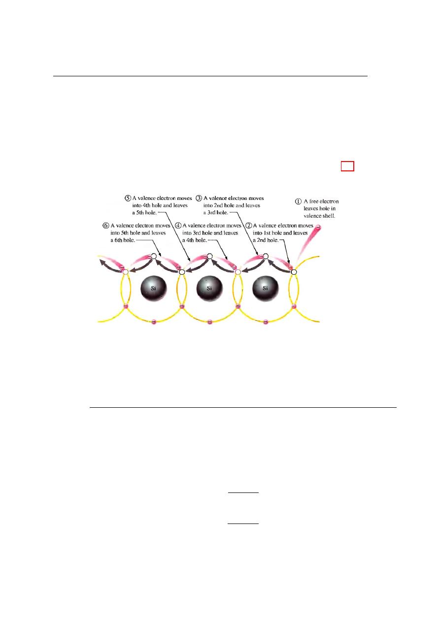
Generation = break up of covalent bond to form electron and hole pairs. A pure
silicon crystal at room temperature derives heat (thermal) energy from the surrounding
environment, causing some valence electrons to gain sufficient energy to jump the gap
from valence band into the conduction band, becoming free electrons. When an electron
jumps to C.B., a vacancy is left in the valence band. This vacancy is called a hole.
If n and p is the free electron and hole concentration, respectively, per volume unit,
Figure 2.3: Free charge carrier generation in semiconductor
at equilibrium status n=p=n
i
. Where n
i
is the carrier concentration. Recombination
occurs when a conduction-band electron loses energy and falls back into a hole in the
valence band.
To summarise, a piece of intrinsic semiconductor at room temperature has, at any in-
stant, a number of conduction-band (free) electrons that are unattached to any atom and
are essentially drifting randomly throughout the material. There is also an equal number
of holes in the valence band created when these electrons jump into the conduction band.
Electron and Hole Current
When a voltage is applied across a piece of intrinsic silicon the thermally generated
free electrons in the conduction band, which are free to move randomly in the crystal
structure, are now easily attracted toward the positive end. This movement of free
electrons is one type of current in a semiconductor material and is called electron current.
26
Transport Phenomena in Semiconductor
Another type of current occurs in the valence band, where the holes created by the free
electrons exist. Electrons remaining in the valence band are still attached to their atoms
and are not free to move randomly in the crystal structure as are the free electrons.
However, a valence electron can move into a nearby hole with little change in its energy
level. thus leaving another hole where it came from. Effectively the hole has moved
from one place to another in the crystal structure. as illustrated in Figure 2.4 This is
called hole current.
Figure 2.4: Hole current in intrinsic silicon
2.4.1
Electrons and Holes Density in an Intrinsic Semiconductor
In a pure (intrinsic) semiconductor the number of holes is equal to the number of
free electrons and the electrical properties determined by host martial. In intrinsic
semiconductor the carrier concentration can be determined from Fermi-Dirac function
distribution:
n = N
c
exp
−
E
c
− E
f
kT
(2.18)
p = N
v
exp
−
E
f
− E
v
kT
(2.19)
2.4
Generation and Recombination of Charges
27
Where n and p are the electron and hole concentration, respectively. N
c
is the active
level density at C.B. and N
v
is the active level density at V.B. and given by:
N
c
=
2 π m
∗
n
kT
h
2
3/2
and
N
v
=
2 π m
∗
p
kT
h
2
3/2
m
∗
n
: effective mass of electron. m
∗
p
: effective mass of hole.
(Effective mass: When we apply an external force to an electron in a crystal, it may
not respond as if it were a free electron. This is because of the interaction with the
crystal lattice). Then the number of carriers is:
n
i
=
√
n p =
p
N
c
N
v
exp
−
E
c
− E
v
2kT
(2.20)
but E
g
= E
c
− E
v
, then;
n
i
=
√
n p =
p
N
c
N
v
exp
−
E
g
2kT
(2.21)
It can be observed that the concentration of electrons and holes in pure semiconductor
independent on the location of the Fermi level but it is depending on the temperature.
2.4.2
Electrons and Holes Density in an Extrinsic Semiconductor
Semiconductor materials do not conduct current well and are of limited value in their
intrinsic state. This is because of the limited number of free electrons in the conduction
band and holes in the valence band. Intrinsic silicon (or germanium) must be modified
by increasing the number of free electrons or holes to increase its conductivity and
make it useful in electronic devices. This is done by adding impurities to the intrinsic
material as you will learn in this section. Two types of extrinsic (impure) semiconductor
materials, n-type and p-type, are the key building blocks for most types of electronic
devices. An extrinsic semiconductor can be formed from adding impurity atoms to
the intrinsic semiconductor in process known as doping. The electrical properties of
extrinsic semiconductor are determined by chemical impurities. For example, silicon
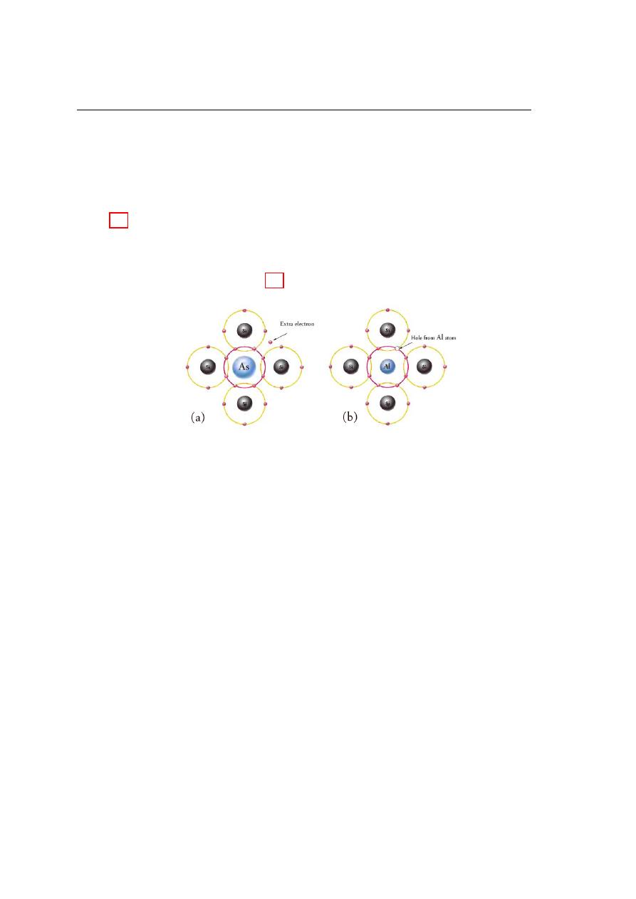
28
Transport Phenomena in Semiconductor
has four valence electrons. Doping silicon with Aluminum (Al) will produce a hole. The
dopant atoms have not enough number of electrons to share bonds with surrounding
silicon atoms. One of the silicon atoms has a vacancy for an electron. It creates hole
that contribute in conduction process and the semiconductor is called p-type as shown in
figure 2.5(a). The dopant atoms are called acceptors. While if the silicon is doped with
Phosphor (P) or Arsenide (As), which they have extra electron in valence bands, the
dopant atoms contributes an additional electron to the crystal and the semiconductor
is called n-type as shown in figure 2.5(b). The dopant atoms are called donors.
Figure 2.5: Extrinsic s.c. (a) n-type s.c. (b) p-type s.c.
Determination of electrons density for n-type semiconductor
If, to intrinsic silicon, there is added a small percentage of phosphor (P ) atoms, a
doped, impure, or extrinsic, semiconductor is formed. The fifth electron of the phosphor
(P ) will be released by energy 0.05eV , which is the smallest energy required an electron
of silicon atom by 20 times (E
g
= 1.1eV ).
Then the density of electron in host semiconductor which doped by N
D
atoms is:
n = N
D
N
D
is the concentration of donor atoms.
The increasing of the electron density in conduction band case shifting in Fermi-
level up word to C.B, then the difference in energy between old and new position of
Fermi-level is:
∆E
n
= E
f n
− E
f i
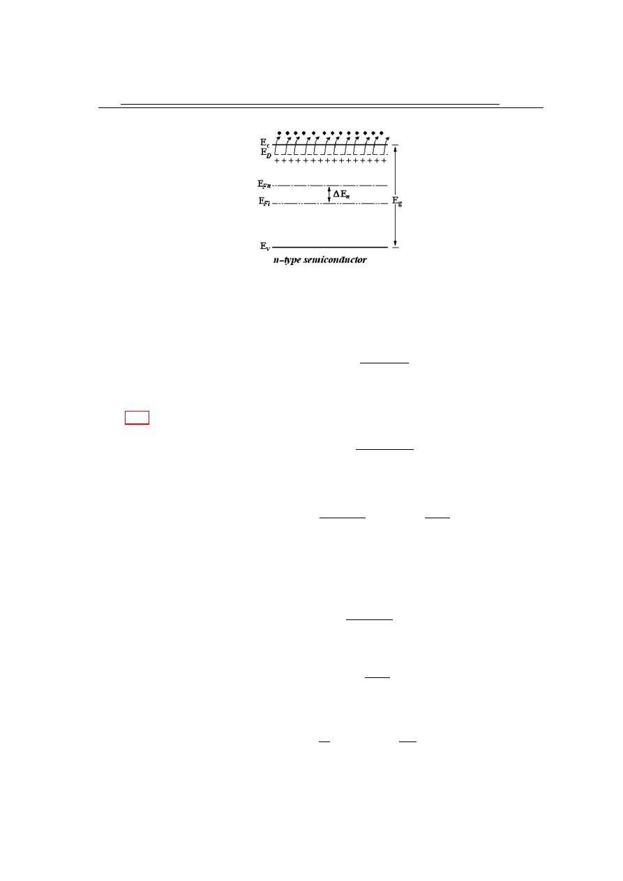
2.4
Generation and Recombination of Charges
29
Figure 2.6: Energy band structure in n-type s.c.
The concentration of the electrons in conduction band is:
n = N
D
= N
c
exp
−
E
c
− E
f n
kT
(2.22)
but, E
f n
= ∆E
n
+ E
f i
then 2.22 becomes;
n = N
D
= N
c
exp
−
E
c
−∆E
n
−E
f i
kT
n = N
D
= N
c
exp
−
E
c
− E
f i
kT
× exp
∆E
n
kT
Since;
n
i
= N
c
exp
−
E
c
− E
f i
kT
then,
n = N
D
= n
i
exp
∆E
n
kT
(2.23)
From the above equation the shift in Fermi level can be calculated as:
∆E
n
= kT ln
n
n
i
= kT ln
N
D
n
i
(2.24)
30
Transport Phenomena in Semiconductor
Determination of holes density of n-type semiconductor The shifting of Fermi
level by ∆E
n
up word in the n-type semiconductor, as shown in figure 2.6, means the
new Fermi level shift away from valance band, and this will cause a new concentration
of holes. Since the hole density given as:
p = N
v
exp
−
E
f n
− E
v
kT
(2.25)
but, E
f n
= ∆E
n
+ E
f i
then 2.25 becomes;
p = N
v
exp
−
E
f i
− E
v
+ ∆E
n
kT
p = N
v
exp
−
E
f i
− E
v
kT
× exp
−
∆E
n
kT
Since;
n
i
= N
v
exp
−
E
f i
− E
v
kT
then,
p = n
i
exp
−
∆E
n
kT
(2.26)
It can be observe that the hole density decrease with Fermi level shifting upward:
n p = n
2
i
Since n = N
D
, then;
p = n
2
i
/N
D
Determination of holes density for p-type semiconductor The doping solid
is the aluminum (Al ) or boron (B), which have 3 valence electrons only, so the doping
atom need one additional electron to bonded with the silicon structure, in this case it’s
can be filled from the nearest bond electrons and this will cause break up the bond near
vacancy. The energy which required is (0.05 eV) for the boron (B) atoms, the number
of charge carriers is equal to the number of holes (doping atoms). The impurity atoms
in this case called the acceptors atoms and it’s density is:
p = N
A
where N
A
is the concentration of acceptor atoms.
2.4
Generation and Recombination of Charges
31
The concentration of holes can be determined from Fermi-Dirac function as below:
p = N
v
exp
−
E
f p
− E
v
kT
(2.27)
new position of Fermi-level is:
∆E
p
= E
f i
− E
f p
Figure 2.7: Energy band structure in p-type s.c.
p = N
A
= N
v
exp
−
E
f i
− ∆E
p
− E
v
kT
p = N
v
exp
−
E
f i
− E
v
kT
× exp
∆E
p
kT
Since;
n
i
= N
v
exp
−
E
f i
− E
v
kT
then,
p = n
i
exp
∆E
p
kT
(2.28)
From the above equation the shift in Fermi level can be calculated as:
∆E
p
= kT ln
p
n
i
= kT ln
N
A
n
i
(2.29)
and the number of electrons is equal to:
n =
n
2
i
N
A
32
Transport Phenomena in Semiconductor
.....℘℘℘℘℘℘℘............................................................℘℘℘℘℘℘℘.....
Solved problems
...........................................................................
1. The electron density in pure silicon is 1.45×10
16
m
−3
at 300
o
K.
Find
the electron density when the temperature change to 350
o
K, take E
g
=
1.1eV ?
Solution
n
i1
=
p
N
c
N
v
exp
−
E
g
2kT
1
.....(1
n
i2
=
p
N
c
N
v
exp
−
E
g
2kT
2
.....(2
n
i1
n
i2
=
exp
−
E
g
2kT
1
exp
−
E
g
2kT
2
n
i2
= n
i1
exp
E
g
2kT
1
exp
E
g
2kT
2
n
i2
= n
i1
exp
E
g
2k
1
T
1
−
1
T
2
= 1.45×10
16
exp
1.1
2 × 8.62 × 10
−5
×
1
300
−
1
350
n
i2
= 3.03 × 10
17
m
−3
————————————————
2. Pure semiconductor with energy gap of 1.42 eV and charge carrier den-
sity of 1.79×10
12
m
−3
at 300
o
K.
Determine the position of the Fermi
level with respect of the mid of gap if N
c
= 4.7 × 10
23
m−3.
What is
the value of N
v
?
Solution
Since the charge concentration in pure semiconductor is equal to electron concen-
tration, so:
n = N
c
exp
−
E
c
− E
f
kT
2.4
Generation and Recombination of Charges
33
E
c
− E
f
= kT ln
N
c
n
=
1.38 × 10
−23
1.6 × 10
−19
× 300 × ln
4.7 × 10
23
1.79 × 10
12
= 0.68 eV
The Fermi level located at 0.68 eV under the E
c
, but the mid of the energy gap
at 0.71 eV under the E
c
. Therefore the position of Fermi level would be 0.03 eV
above the mid of the gap.
** Home work ⇒ Find N
v
**
————————————————
3. Pure silicon has electron concentration 1.45×10
16
m
−3
at 300
o
K was doped
with 10
22
m
−3
phosphor (P ) atoms.
Find the electron and hole densities
at 300
o
K and 500
o
K?
Solution
n
i
= 1.45 × 10
16
m
−3
before doping at 500
o
K the doping solid is phosphor (P )
which is donor atoms, then; n = N
D
= 10
22
m
−3
the density of the solid after
doping at 300
o
K
n
i1
n
i2
=
exp
−
E
g
2kT
1
exp
−
E
g
2kT
2
n
i2
= n
i1
exp
E
g
2kT
1
exp
E
g
2kT
2
n
i2
= n
i1
×exp
E
g
2k
1
T
1
−
1
T
2
= 1.45×10
16
× exp
1.1
2 × 8.62 × 10
−5
×
1
300
−
1
500
n
i2
= 7.2 × 10
19
m
−3
p
2
=
n
2
i2
N
D
= 5.2 × 10
17
m
−3
————————————————
4. The electron concentration in pure silicon is 1.5×10
16
m
−3
at 300
o
K.
The silicon was doped with 10
22
m
−3
donor atoms.
Find the electron and
hole densities after doping and calculate the position of the new Fermi
level with to the initial position?
34
Transport Phenomena in Semiconductor
Solution
After doping the density of electron is n = N
D
= 10
22
m
−3
, while the hole density
is given as;
p =
n
2
i
N
D
=
1.5 × 10
162
10
22
= 2.25 × 10
10
m
−3
∆E
n
= kT ln
N
D
n
i
∆E
n
=
1.38 × 10
−23
1.6 × 10
−19
× 300 × ln
10
22
1.5 × 10
16
= 0.347 eV
The new position of Fermi level is above the initial position by 0.347 eV
————————————————
5. If the position of Fermi level in impure semiconductor at 0.3 eV above
the mid of the energy gap at 300
o
K, where the E
g
= 1.1 eV and n
i
=
1.45 × 10
16
m
−3
.
What is type of the impurities and what are its concentration?
Solution
Since the Fermi level location is above the mid of the energy gap, therefore the
semiconductor would be from n-type. So the impurities are donor atoms.
N
D
= n
i
× exp
∆E
n
kT
N
D
= 1.45 × 10
16
× exp
0.3
8.614 × 10
5
× 300
= 1.58 × 10
21
m
−3
2.5
Electrical conduction in semiconductor
As it was seen that the electron motion and the electrical conduction in metal depend
on several parameters which describe the electrical motion in metal, this description for
the electron motion and the electrical conduction is same to these in semiconductor but
with take care the ratio of doping.
2.5
Electrical conduction in semiconductor
35
2.5.1
Electrical conduction in intrinsic semiconductor
The electrical conduction in intrinsic semiconductor is same the general formula of
conductivity in metal:
σ = n e µ
Applied this formula on an intrinsic semiconductor, the electrons and holes contribute
in electrical conduction then:
σ
i
= n e µ
n
+ p e µ
p
(2.30)
where;
n=concentration of electrons (m
−3
)
µ
n
=electron mobility (m
2
V
−1
s
−1
)
p=concentration of holes (m
−3
)
µ
p
=hole mobility (m
2
V
−1
s
−1
)
In pure semiconductor the concentration of electrons equal to concentration of holes;
i.e., p=n=n
i
, then equation 2.30 can be written as;
σ
i
= n
i
e (µ
n
+ µ
n
)
(2.31)
and n
i
is;
n
i
=
p
N
c
N
v
exp
−
E
g
2kT
n
i
=
s
2π m
∗
n
k T
h
2
3/2
×
2π m
∗
p
k T
h
2
3/2
×
exp
−
E
g
2kT
n
i
=
2π k
h
2
3/2
×
m
∗
n
m
∗
p
3/4
× T
3/2
×
exp
−
E
g
2kT
n
i
∝ T
3/2
×
exp
−
E
g
2kT
36
Transport Phenomena in Semiconductor
Since it is known that;
µ
n
=
e t
n
m
∗
n
and
µ
p
=
e t
p
m
∗
p
where, t
n
and t
p
are the relaxation time of electrons and holes respectively.
The mobility depends on the relation time and effective mass of moving charges.
Heating the semiconductor causes vibration of atoms and this will effect on electron
motion inside the crystal structure and hence the electrons collision with atoms will
increase due to vibration of atoms and therefore the mobility will decreases.
µ ∝ T
−3/2
Then it can be conclude that:
σ ∝ n
i
=⇒ σ ∝ T
3/2
×
exp
−
E
g
2kT
and;
σ ∝ µ =⇒ σ ∝ T
3/2
As a result of that the semiconductor conductivity affected by temperature as:
σ
i
= σ
o
exp
−
E
g
2kT
(2.32)
where, σ
o
is a constant and independent to temperature. Equation 2.32 can also be
written as:
ln (σ
i
) = ln (σ
o
) −
E
g
2kT
The semiconductor conductivity changes strongly with temperature variation.
1
σ
i
dσ
i
dT
= −
E
g
2kT
(2.33)
2.6
Diffusion and Drift currents density in semiconductor
37
2.5.2
Electrical conduction in extrinsic semiconductor
When the semiconductor is doped by impurities has N
D
concentration (n >> p):
σ
(n)
= n e µ
n
+ p e µ
p
(2.34)
In other words equation 2.34 can be written as;
σ
(n)
= σ
n
+ σ
p
But n × p = n
2
i
=⇒ N
D
× p = n
2
i
=⇒ p = (n
2
i
/N
D
), then equation 2.34 can also be
written as;
σ
(n)
= N
D
e µ
n
+
n
2
i
N
D
e µ
p
(2.35)
∵ N
D
= n >> n
i
that is meaning the p concentration has no effect and (σ
n
>> σ
p
), so:
σ
(n)
= N
D
e µ
n
In the same manner if the semiconductor is doped by impurities have
N
A
acceptor atoms concentration (N
A
= p >> n
i
): σ
(p)
= N
A
e µ
p
2.6
Diffusion and Drift currents density in semiconductor
There are two mechanisms by which holes and electrons move through a silicon
crystal diffusion and drift.
Diffusion current density:
As aforementioned the diffusion current density is
given as:
J
dif f
= −e D
dn
dx
(2.36)
Since the diffusion current density in semiconductor is due to electrons and holes
motion, then:
J
dif f
= J
dif f (n)
+ J
dif f (p)
= −e
D
n
dn
dx
+ D
p
dp
dx
(2.37)
Drift current density: As aforementioned the drift current density is given as:
J
d
= −e n µ
n
(2.38)
38
Transport Phenomena in Semiconductor
The free electrons will drift in the direction opposite to that of E. The total drift
current density is obtained by combining the two charge carriers:
J
drif t
= J
d
= e E (n µ
n
+ p µ
p
)
(2.39)
2.7
Photo-conductivity
When the semiconductor exposure to electromagnetic wave has energy (hf ) then
this energy will cause a generation of a new charge carriers contribute in electrical
conduction process, this called the Photo-conductivity: If the energy of exposure photon
is: hf ≥ E
g
. In other words the minimum wavelength of the absorbed electromagnetic
radiation which can produce a new charge carriers will given as:
λ ≤
1.24
E
g
(µm)
(2.40)
The ability of the semiconductor to absorb photons depend on its nature and fre-
quency. If the semiconductor surface exposure to the ray of the photons n
ph(o)
, so the
number of the photons will decrease with penetration depth (x) of the surface and the
number of the photons which will arrive to depth (x) would be:
n
ph(x)
= n
ph(o)
.exp (−αx)
(2.41)
α : is the absorption constant. α proportion to the absorption of solid ability to photons,
so if α is large the solid has good ability to absorb.
2.7
Photo-conductivity
39
Solved problems
1. Pure germanium has (4 × 10
22
) atom. cm
−3
doped by indium atoms, the
impurity is add to the extent of 1 part in (10
8
) germanium atoms, if
the intrinsic concentration of germanium 2.5 × 10
13
cm
−3
, note that
µ
n
= 3800 cm
2
(V s)
−1
and µ
p
= 1800 cm
2
(V s)
−1
.
(a) Find the conductivity and the resistivity before the doping?
(b) Find the conductivity and the resistivity after the doping?
(c) What can you conclude from 1 and 2?
Solution
1. The conductivity of pure semiconductor (before doping) is given by:
σ = neµ
n
+ peµ
p
since the semiconductor is intrinsic then, n = p = n
i
σ = n
i
e (µ
n
+ µ
p
)
σ = 2.5 × 10
13
× 1.6 × 10
−19
× (3800 + 1800) = 0.0224 S cm
−1
ρ =
1
σ
ρ =
1
0.0224
= 44.64 Ω cm
2. Doping pure germanium with indium will produce increasing in hole density,
so:
N
A
=
4 × 10
22
10
8
= 4 × 10
14
cm
−3
n × p = n
2
i
⇒ n × N
A
= n
2
i
⇒ n =
n
2
i
N
A
n =
(2.5 × 10
13
)
2
4 × 10
14
= 1.56 × 10
12
cm
−3
40
Transport Phenomena in Semiconductor
(2.5 × 10
3
)
2
10
14
σ = neµ
n
+ peµ
p
σ = 1.6 × 10
−19
× 1.56 × 10
12
× 3800 + 4 × 10
14
× 1800
= 0.116Scm
−1
ρ =
1
σ
=
1
0.116
= 8.62Ωcm
3. The ratio between the conductivity after and before doping is given as:
σ
(af ter doping)
σ
(bef ore doping)
=
0.116
0.0224
= 5.18
The conductivity of the germanium increased more than 5 time after doping with
indium.
2. Pure silicon doped by antimony has concentration equal to
2 × 10
15
atom. cm
−3
, until N
D
− N
A
2n
i
, note that they represent
replacement of less than 10
−5
% of the atoms in the silicon.
Find
the conductivities
σ
(n)
, σ
(p)
and σ
and the resistivity ρ of the
silicon?
note that µ
n
= 1260 cm
2
(V s)
−1
and µ
p
= 460 cm
2
(V s)
−1
.
Solution
When the pure silicon doped with antimony atoms mean doping by donor atoms:
N
D
= 2 × 10
15
atom cm
−3
∴ 10
−5
× 2 × 10
15
− 0 2n
i
n
i
= 10
10
atom cm
−3
n.p = n
2
i
p N
D
= n
2
i
=⇒ p = (n
2
i
)/N
D
p = (10
10
)
2
/(2 × 10
15
) = 5 × 10
4
atoms cm
−3
σ
n
= N
D
e µ
n
= 2 × 10
15
× 1.6 × 10
−19
× 1260 = 0.403 S cm
−1
σ
p
= p e µ
p
= 5 × 10
4
× 1.6 × 10
−19
× 460 = 368 × 10
−14
S cm
−1
σ = σ
n
+ σ
p
2.8
Hall Effect
41
∵ σ
n
σ
p
∴ σ = σ
n
σ = 0.403 S cm
−1
ρ =
1
σ
=
1
0.403
= 2.48 Ω cm
2.8
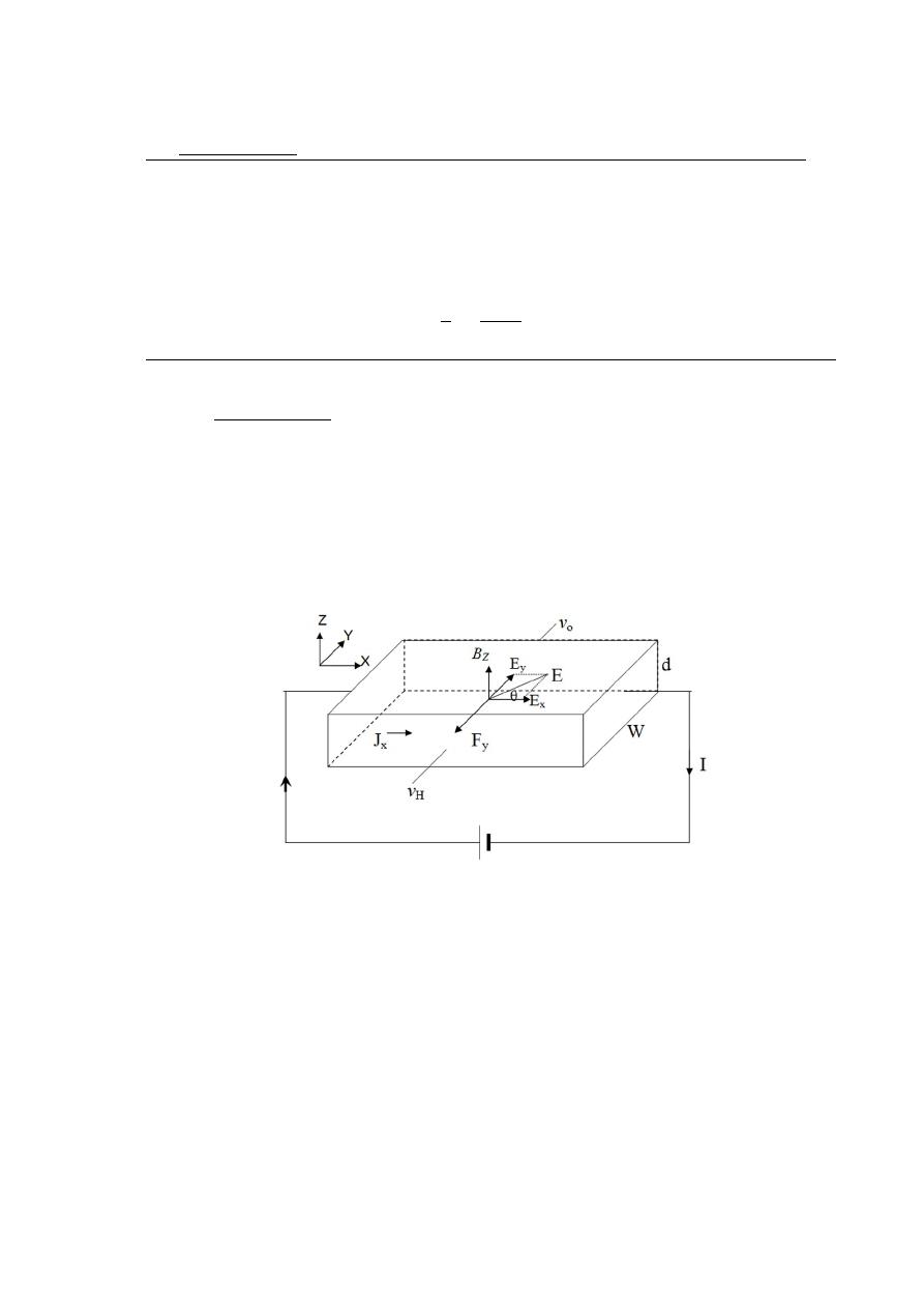
Hall Effect
Suppose that an electric current J
x
is flow in a semiconductor in the x-direction,
and a magnetic field B
z
is applied normal to the s.c. in the z-direction. The current
J
x
will cause from the motion of holes (if the s.c. from p-type) with speed v
Dx
under
the influence the electric field E
x
. These holes will effect to force F
L
known as Lorentz
Force and in (−y) direction as shown in Figure below.
Figure 2.8: Hall effect setup
F
L
= e × v
Dx
× B
z
(2.42)
This force will push the holes in the front surface direction; this will cause a high
density of holes on this surface while the back surface would be empty from the holes.
Since the flow of hole current in y-direction (E
y
). This field cause from the distribution
of holes, and the field will cause a force on holes equal to Lorentz force, i.e.:
42
Transport Phenomena in Semiconductor
e E
y
= e × v
Dx
× B
z
(2.43)
but
J
x
= e × v
Dx
× p
E
y
=
J
x
B
z
p e
(2.44)
or,
1
p e
=
E
y
J
x
B
z
The quantity
1
p e
called Hall Coefficient (R
H
), then;
R
H
=
1
p e
=
E
y
J
x
B
z
(2.45)
The induced potential between front and back surfaces can be measured and then;
V
H
= E × W
If the thickness of the slide is d then,
I = J
x
× W × d
Substituting the value of J
x
in equation 2.45, then:
R
H
=
V
H
d
I B
z
=
1
p e
(2.46)
Since V
H
, d I, and B
Z
are a measurable values, then it can be calculated the Hall
coefficient experimentally and hence calculated the hole concentration from equation
2.46. Similar analysis can be done for a semiconductor of n-type and find:
R
H
=
1
n e
(2.47)
It is seen in last figure that there is a result of electrical field (E) in (θ) direction
about the direction of (E
x
), then,
2.8
Hall Effect
43
tanθ =
E
y
E
x
(2.48)
Substituting the value of (E
y
) from equation 2.46 in equation 2.48, then it can find,
tanθ =
J
x
B
z
p e
×
σ
J
x
= µ
p
B
z
(2.49)
or,
µ
p
= R
H
σ
(2.50)
According to this simple analysis it can measured the mobility of hole from Hall coeffi-
cient and conductivity.
Solved problems
1. A current of (0.12 A) pass through n-type semiconductor have a width of
(w = 2 mm) and thickness of (d = 1 mm).
If the voltage along the
width of this sample of semiconductor is (3.4 mV ) and a normal magnetic
field of (500 Gauss) applied on this piece of semiconductor, find the
Hall coefficient and electron density?
Solution
R
H
=
V
H
× d
I × B
z
R
H
=
3.4 × 10
−3
× 1 × 10
−3
0.12 × 500 × 10
−4
= 5.6 × 10
−4
m
3
C
−1
R
H
=
1
n e
5.6 × 10
−4
=
1
n × 1.6 × 10
−19
⇒ n = 2 × 10
22
m
−3
44
Transport Phenomena in Semiconductor
2. Find the Hall coefficient, electron density and the angle between the
field components for n-type semiconductor wire having thickness of (d =
2 mm)?
The normal applied magnetic field on this semiconductor is (B =
0.1 T ) and the current which passing through it is (10 mA), and (V
H
=
1 mV ), (µ
n
= 0.36 m
2
s
−1
).
Solution
R
H
=
V
H
× d
I × B
z
R
H
=
1 × 10
−3
× 2 × 10
−3
10 × 10
−3
× 0.1
= 2 × 10
−3
m
3
C
−1
R
H
=
1
n e
2 × 10
−3
=
1
n × 1.6 × 10
−19
⇒ n = 3.1 × 10
21
m
−3
tanθ = µ
p
B
z
= 0.36 × 0.1 = 0.036 ⇒ θ = tan
−1
(0.036) = 2
o
2.8
Hall Effect
45
Review Questions
1.
Define mobility? Give its dimensions?
2. Indicate pictorially how a hole contributes to conduction?
3. (a) Define intrinsic concentration of holes. (b) What is the relationship between this
density and the intrinsic concentration for electrons? (c) What do these equal at 0
o
K?
4. Given an intrinsic semiconductor specimen, state two physical processes for increasing
its conductivity? Explain briefly.
5. Explain physically the meaning of the following statement: An electron and a hole
recombine and disappear?
6. Define (a) donor, (b) acceptor impurities?
7. What properties of a semiconductor are determined from a Hall effect experiment?
8. A pure silicon contains 5 × 10
28
atom per cubic meter and the ratio of broken bonds are
one bond per 10
12
silicon atom at 38
o
C. What is the ratio of broken of covalent bonds
if the temperature raised to 75
o
C, where E
g
= 1.1 eV ?
9. A piece of pure semiconductor contains 5×10
18
donor atoms at 27
o
C. How far the Fermi
level will move and in which direction if an additional donor atoms of concentration of
10
22
will put in?
10. What is the wavelength of the electromagnetic waves which can release an electron from
Germanium and Silicon? where E
g
(Ge) = 0.66 eV and E
g
(Si) = 1.1 eV .
11. The charge carriers concentration in pure silicon is 4.5 × 10
16
m
−3
at 300
o
K. Where the
Fermi level would be if the silicon doped by 1 × 10
21
donor atoms? Find the location of
Fermi level at 200
o
K and 900
o
K. Use E
g
(Si) = 1.1 eV .
12. If the conductivity of the pure Germanium change with temperature according the fol-
lowing relation, so what is the energy gap of the Germanium?
exp
−4350
T

46
Transport Phenomena in Semiconductor
13. A resistor of pure Silicon with a resistance of 2500 Ω at 20
o
C, if the resistance of this
resistor increased by 1% of its initial vaule when the temperature increased to 100
o
C,
what is the energy gap of Silicon?
14. The resistivity of pure Silicon doped with impurities is 9.27 × 10
−7
Ω m and the Hall
coefficient is 3.84 × 10
−4
m
3
C
−1
, what is the density and the mobility of impurities
atoms?
============
Chapter 3
P-N Junction (Diode)
—————————————————————————————————–
If one side of a piece of silicon dope with a trivalent impurity and the
other side with a pentavalent impurity, a (p − n) junction will formed be-
tween the resulting p-type and n-type portions and a basic diode will cre-
ated. A diode is a device that conducts current in only one direction. In
this chapter we demonstrate the characteristics of the (p − n) junction re-
gion. The volt-ampere characteristics of the (p−n) junction is studied. The
capacitance across the junction is calculated.
——————————————————————————————————
3.1
The structure of p-n junction
If a donor impurities are doped into one side and acceptors into the other side of a
single crystal of a pure semiconductor, a (p − n) junction will create. This two-terminal
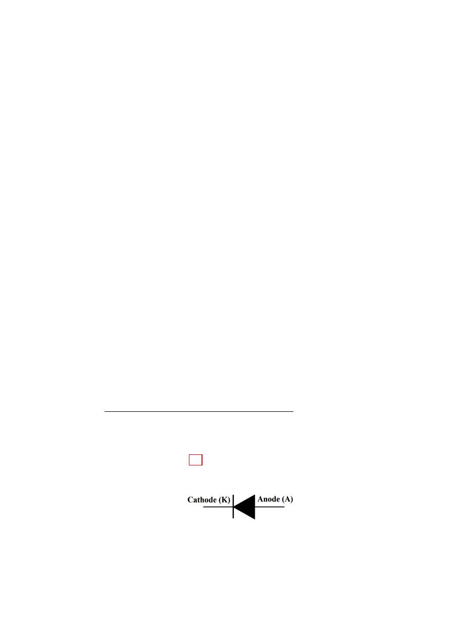
device called a junction diode. 3.1 Fig.(1) shows the schematic symbol of the diode. The
key feature of this device that conducts current in only one direction. When the n-type
Figure 3.1: Diode schematic symbol.
48
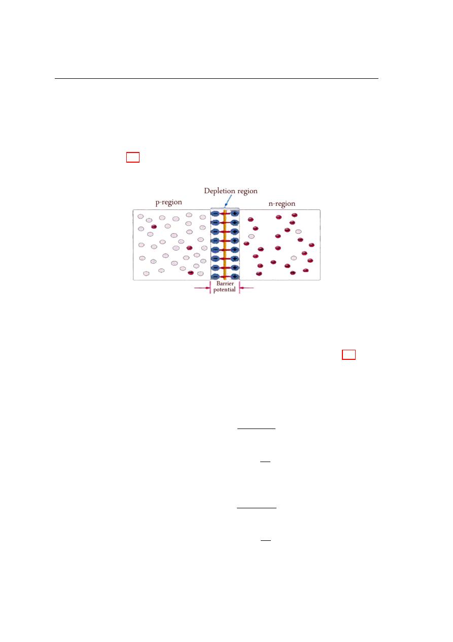
P-N Junction (Diode)
semiconductor connect to p-type semiconductor the n region loses free electrons as they
diffuse across the junction. This creates a layer of positive ions near the junction. The
p region loses holes as electrons and holes combine. This creates a layer of negative ions
near the junction. These two layers of positive and negative form the depletion region,
as shown in figure3.2, with a built-in potential which is called the contact or barrier
potential (V). The depletion region is completely free from the charges.
Figure 3.2: Formation of the depletion region.
From the basic conception of the semiconductor, it is easy to determine the value
of the barrier or contact potential . From the energy levels in figure 3.3 it can be
observed that:
E
cp
− E
cn
= e V
o
In p-side, the electron concentration as a minor charge carrier is given as:
n
p
= N
c
× exp
−
E
cp
− E
f p
kT
E
cp
= E
f p
− kT × ln
n
p
N
c
whilst the electron concentration as a major charge carrier in n-side is given as:
n
n
= N
c
× exp
−
E
cn
− E
f n
kT
E
cn
= E
f n
− kT × ln
n
n
N
c
3.1
The structure of p-n junction
49
Figure 3.3: The P-N junction and its energy levels after contacted.
and
eV
o
= E
cp
− E
cn
∴ eV
o
=
E
f p
− kT × ln
n
p
N
c
−
E
f n
− kT × ln
n
n
N
c
]
Since the junction is in equilibrium status, then:⇒ E
f p
= E
f n
, then it can be write:
V
o
=
kT
e
ln
n
n
n
p
(3.1)
Equation 3.1 can also be written as;
n
n
= n
p
× exp
eV
o
kT
Since n
n
= N
D
and n
p
= n
2
i
/N
A
, then the above equation becomes:
V
o
=
kT
e
ln
N
D
× N
A
n
2
i
(3.2)
In same way, from n-side it could be found;
V
o
=
kT
e
ln
p
p
p
n
or p
p
= p
n
× exp
eV
o
kT
50
P-N Junction (Diode)
Solved problems
1. A pn junction was formed from two pieces of silicon contain N
D
= 10
24
m
−3
and N
A
= 10
20
m
−3
at 300
o
K.
Find the barrier potential?
The carrier
concentration for pure silicon is:
n
i
= 1.45 × 10
16
m
−3
.
Solution
V
o
=
kT
e
× ln
N
D
× N
A
n
2
i
=
1.38 × 10
−23
× 300
1.6 × 10
−19
× ln
10
24
× 10
20
(1.45 × 10
16
)
2
= 0.7 volt
2. A pure silicon has n
i
= 1.45×10
16
m
−3
, doped in its two ends by phos-
phor (P ) and Boron (B) with carrier densities N
D
= 10
22
m
−3
and N
A
=
10
20
m
−3
, respectively to form a p-n junction at 300
o
K.
Find:
(a) The location of Fermi-level in n and p parts?
(b) Determine the barrier potential?
Solution
(a) For n-side
N
D
= n
i
× exp
E
f n
− E
f i
kT
∴ E
f n
− E
f i
= kT × ln
N
D
n
i
=
1.38 × 10
−23
× 300
1.6 × 10
−19
× ln
10
22
(1.45 × 10
16
)
= 0.35 eV above F ermi level
(b) For p-side
N
A
= n
i
× exp
E
f i
− E
f p
kT
∴ E
f i
− E
f p
= kT × ln
N
A
n
i
=
1.38 × 10
−23
× 300
1.6 × 10
−19
× ln
10
20
(1.45 × 10
16
)
= 0.27 eV below F ermi level
V
o
=
kT
e
×ln
N
D
× N
A
n
2
i
=
1.38 × 10
−23
× 300
1.6 × 10
−19
×ln
10
22
× 10
20
(1.45 × 10
16
)
2
= 0.62 volt
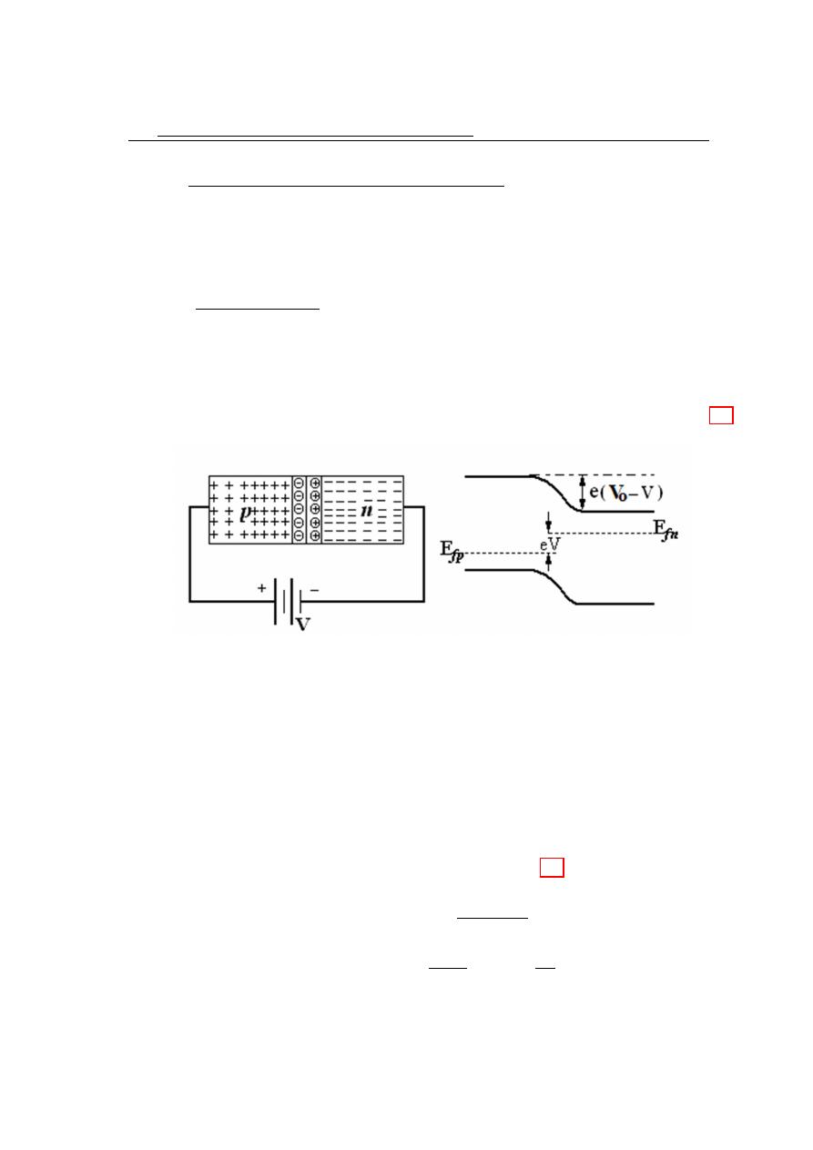
3.2
PN junction characteristics
51
3.2
PN junction characteristics
If the external potential of V volt is applied across the P-N junction this will bias
the diode. There are two type of diode bias:
3.2.1
Forward bias
Connecting an external voltage across the junction will cause a disturbance in the
junction equilibrium status and a net current will flow through the P-N junction. Con-
necting the positive terminal of the external voltage source to the p-side and the negative
terminal to the n-type will cause a forward bias for the junction as shown in figure 3.4.
Figure 3.4: Forward bias voltage (V) applied to p-n junction and the result energy band
structure.
The application of forward bias potential V will cause an injection of electrons from
n-side and hole from p-side in opposite direction across the junction region and some
of these carriers will recombine with the ions near the boundary region and reduce
the width of depletion region. On being injected across the junction, these carriers
immediately become minority carriers and the density of the minority carriers near the
junction rise to new values n
po
and p
no
. as shown in figure 3.4.
n
po
= n
n
× exp
−
e (V
o
− V )
kT
(3.3)
n
po
= n
n
× exp
−
e (V
o
)
kT
× exp
eV
kT
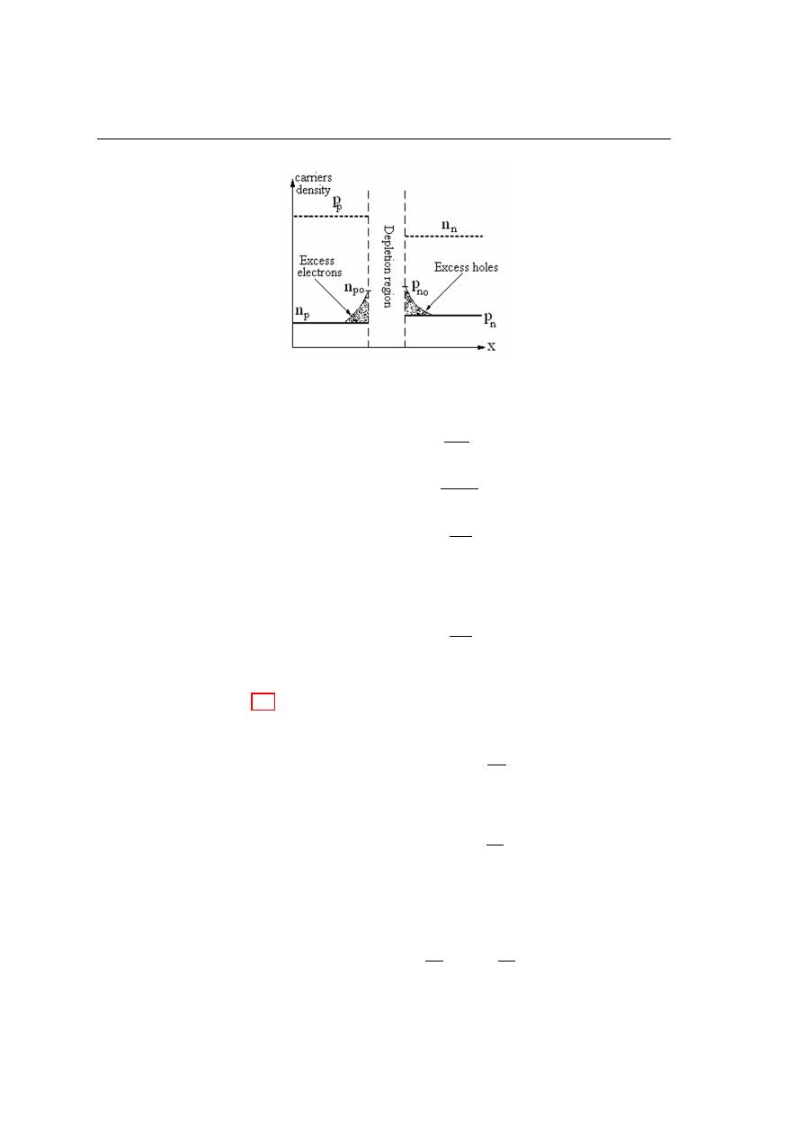
52
P-N Junction (Diode)
Figure 3.5: The excess carriers in the terminals of junction.
∵ n
n
= n
p
× exp
e V
o
kT
So n
p
= n
n
× exp
−e V
o
kT
∴ n
po
= n
p
× exp
e V
kT
(3.4)
where n
po
is the electrons excess at the edge of the depletion region in p side.
In same manner it can be prove that:
∴ p
no
= p
n
× exp
e V
kT
(3.5)
where p
no
is the electrons excess at the edge of the depletion region in n side.
As shown in figure 3.5, the density of carrier decreases far from the depletion region
to exist the forward bias.
n(x) = n
p
− (n
p
− n
po
) exp
−
x
L
n
(3.6)
L
n
:the electron diffusion length in p-side.
p(x) = p
n
− (p
n
− p
no
) exp
−
x
L
p
(3.7)
L
p
:the electron diffusion length in n-side.
The total current densities are due to holes and electrons diffusion motion is defined
as:
J
D
= J
n
+ J
p
= e D
n
dn
dx
+ e D
p
dp
dx
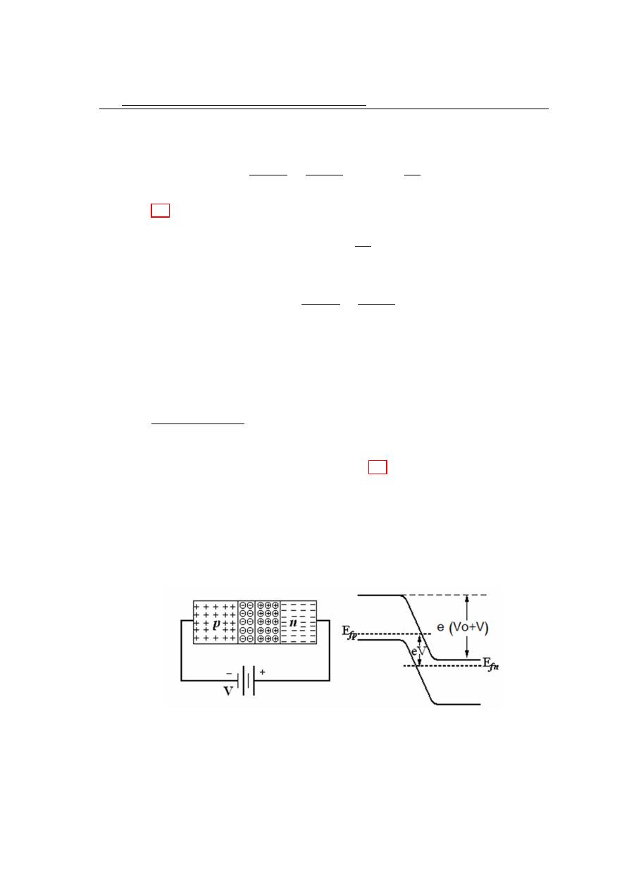
3.2
PN junction characteristics
53
with caring to the direction of (x), then the above equation can be written as:
J
D
=
e D
n
n
p
L
n
+
e D
p
p
n
L
p
×
exp
eV
kT
− 1
(3.8)
Equation 3.8 can be written as;
J
F
= J
s
×
exp
eV
kT
− 1
(3.9)
where;
J
s
=
e D
n
n
p
L
n
+
e D
p
p
n
L
p
The value J
s
represents the saturation current density, whilst J
F
the forward current
density. Saturation current flows through the junction in equilibrium case between the
diffusion currents under the effect of (V
o
).
3.2.2
Reverse bias
If the positive terminal of the applied voltage connect to the n−type and the negative
terminal to the p − type, as illustrated in figure 3.6, the junction will bias in reverse
direction. Because unlike charges attract, the positive side of the bias-voltage source
”pulls” the free electrons, which are the majority carriers in the n region, away from
the pn junction. As the electrons flow toward the positive side of the voltage source,
additional positive ions are created. This results in a widening of the depletion region
and a depletion of majority carriers. In the p region, electrons from the negative side
Figure 3.6: A (p-n) junction under the reverse bias and the equivalent energy band
structure.
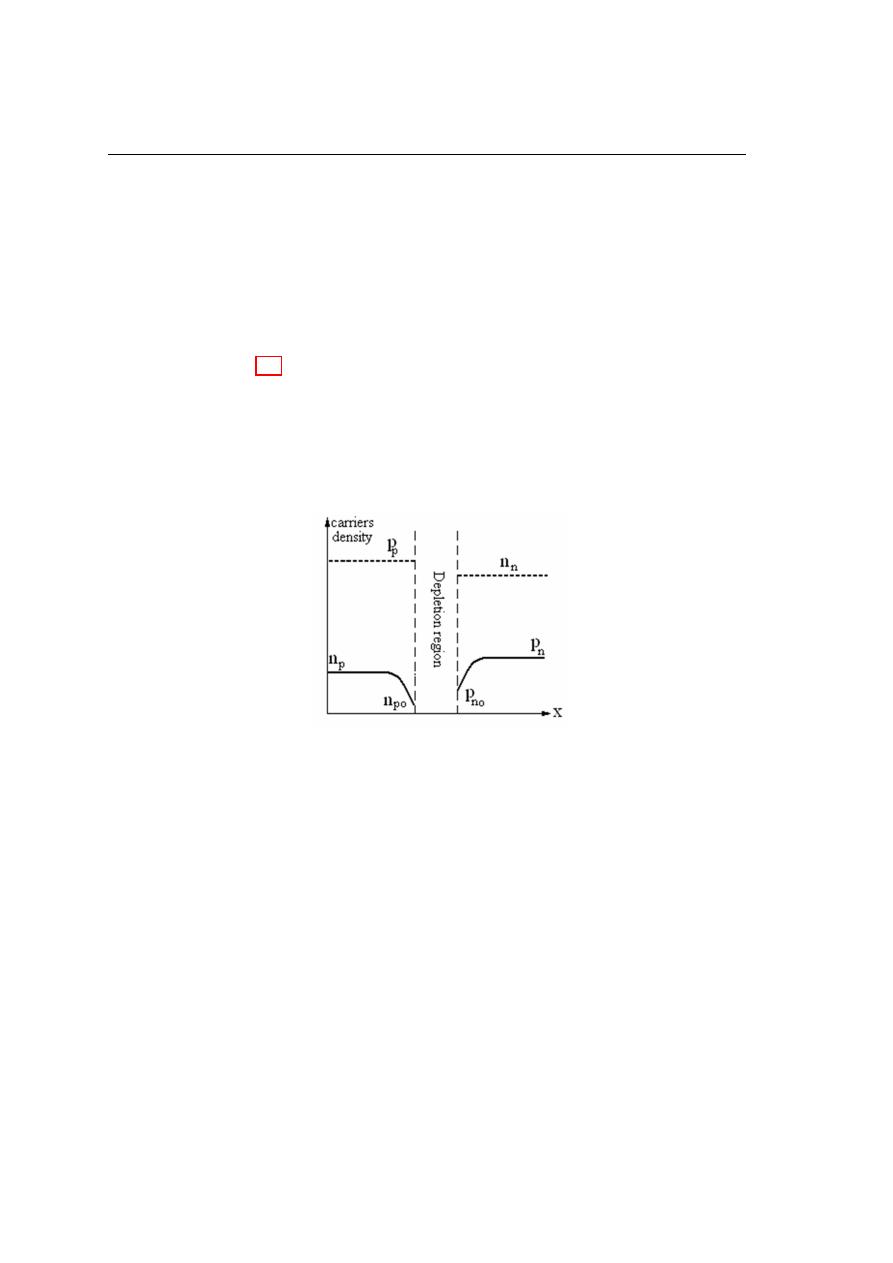
54
P-N Junction (Diode)
of the voltage source enter as valence electrons and move from hole to hole toward the
depletion region where they create additional negative ions. This results in a widening
of the depletion region and a depletion of majority carriers. The flow of valence electrons
can be viewed as holes being ”pulled” toward the positive side. The initial flow of charge
carriers is transitional and lasts for only a very short time after the reverse-bias voltage
is applied. As the depletion region widens, the availability of majority carriers decreases
as shown in figure 3.7. As more of the n and p regions become depleted of majority
carriers, the electric field between the positive and negative ions increases in strength
until the potential across the depletion region equals the bias voltage, V
bias
. At this
point. The transition current essentially ceases (dies) except for a very small reverse
current that can usually be neglected. Reverse Current: The extremely small current
Figure 3.7: The carrier densities in bulk of reverse bias p-n junction.
that exists in reverse bias after the transition current dies out is caused by the minority
carriers in the n and p regions that are produced by thermally generated electron-hole
pairs. The small number of free minority electrons in the p region are ”pushed” toward
the pn junction by the negative bias voltage. When these electrons reach the wide
depletion region, they ”fall down the energy hill” and combine with the minority holes
in the n region as valence electrons and flow toward the positive bias voltage, creating
a small hole current. The conduction band in the p region is at a higher energy level
than the conduction band in the n region. Therefore, the minority electrons easily pass
through the depletion region because they require no additional energy. The current in
reverse-bias condition called Reverse Saturation Current (I
s
).
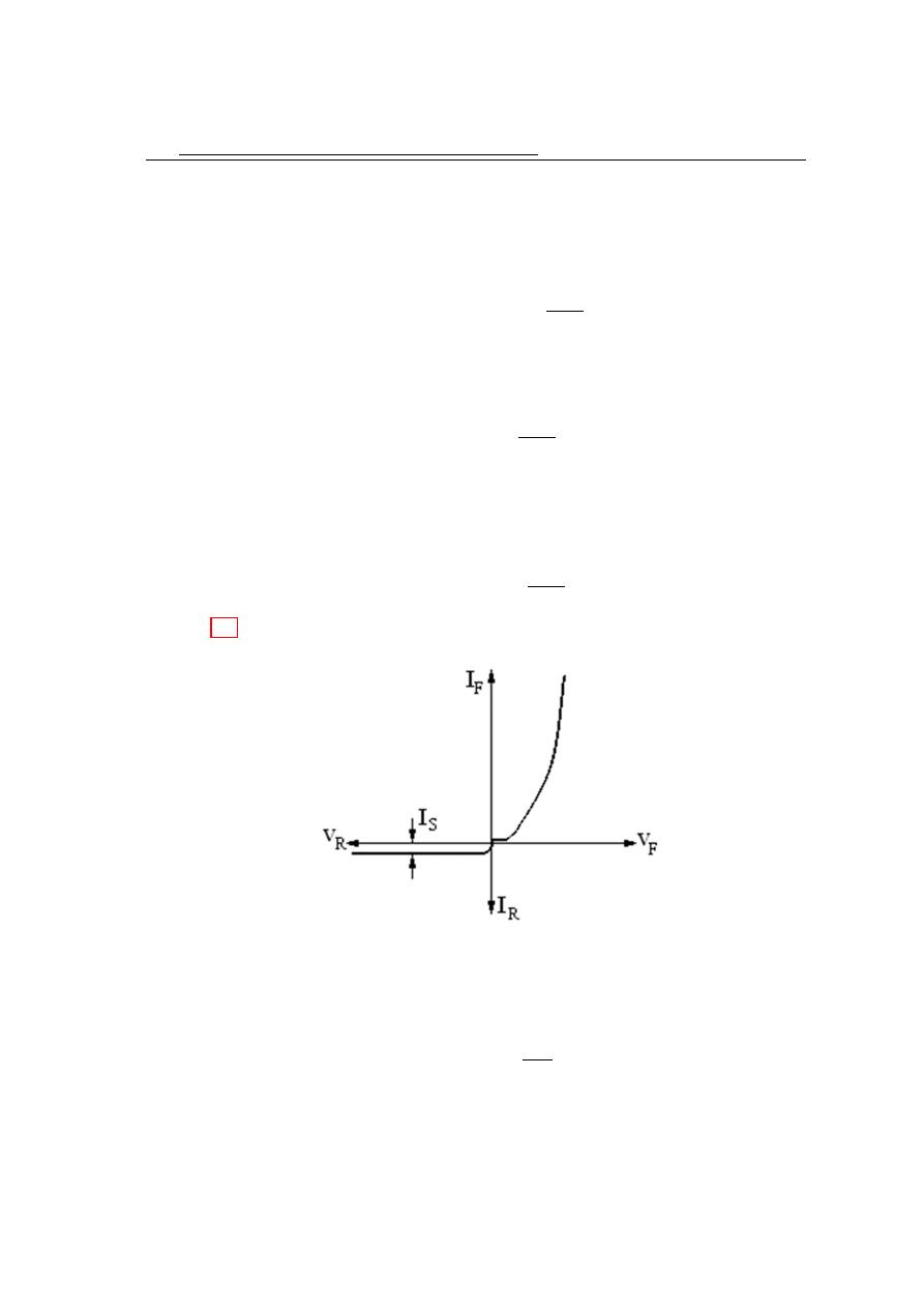
3.2
PN junction characteristics
55
The applied voltage lead to increase the height of barrier potential to a new value
equal to (V
o
+ V ), thereby reducing the diffusion current through the junction. The
current density at reverse bias is given as:
J
R
= J
s
×
1 − exp
−eV
kT
(3.10)
where J
R
is the reverse current density.
The general formula of the current density in the p-n junction can be form as:
J = ± J
s
×
exp
±eV
kT
− 1
(3.11)
where (+):forward and (−):reverse.
If the junction cross-section area is equal to (A)
then the current is:
I = A.J and I
s
= A.J
s
∴ I = ± I
s
×
exp
±eV
kT
− 1
(3.12)
Figure 3.8 shows the relation between the current and voltage in both forward and
Figure 3.8: I − V characteristics of the p − n junction.
reverse biases. For the large values of V
F
, where (V
F
> 4kT ) the forward current is:
I
F
= I
s
exp
eV
F
kT
and for long time the reverse bias (I
R
= I
S
).
56
P-N Junction (Diode)
3.3
Depletion region and depletion capacitances
The two space charge density layers at the junction vary in width with the applied
voltage, and therefore in the amount of charges they contain as the bias voltage changes.
If (w) is the width of the depletion region then:
w = d
n
+ d
p
(3.13)
where (d
n
) with in the n-side and (d
p
) with in the p-side.
It can be related between (d
n
and d
p
) from the charge density in these regions:
N
−
A
A d
p
= N
+
D
A d
n
or
d
p
d
n
=
N
+
D
N
−
A
Since the width of the depletion region effect by biasing voltage then:
w =
2
e
1
N
−
A
+
1
N
+
D
(V
o
± V )
1
2
(3.14)
The −ve sign for the forward bias and +ve sign for the reverse bias. Where =
o
r
.
If the reverse bias at |V
R
| > V
o
and N
A
N
D
or N
D
N
A
;
w =
2 V
R
e N
1
2
(3.15)
N : the impurities concentration for much less type. The depletion region is a free of
charges (carriers), therefore it can be considered as insulator with capacitance.
C
j
=
w
=
r e N
2 V
R
in unit
F
m
2
(3.16)
It can see that the capacitance of depletion region dependent on applied reverse voltage.
C
j
∝ V
−1/2
R
(variable capacitor f or abrupt junction)
C
j
∝ V
−1/2
R
(variable capacitor f or graded junction)
The capacitance property for a pn junction in reverse bias is very useful for IC but
its value variable depend on applied voltage. variable capacitor→Tuning ≡ called
(varactor)
3.4
Diffusion capacitors
57
3.4
Diffusion capacitors
It is very important than the junction capacitor, where it is depend on the density of
minority carriers on the edge of the depletion region. These carriers effect with external
applied voltage (V
F
), then the diffusion capacity is given by:
C
D
=
e
2
2 k T
[p
n
L
p
+ n
p
L
n
] exp
e V
F
k T
(3.17)
Note that;
C
D
∝ exp
e V
F
k T
I
F
= I
S
exp
e V
F
k T
dI
F
dV
F
=
e
k T
× I
S
exp
e V
F
k T
∴
dI
F
dV
F
=
e I
F
k T
=
1
r
d
Multiply equation 3.17 by
I
F
I
F
C
D
=
e I
F
k T
×
e
2 I
F
[p
n
L
p
+ n
p
L
n
] exp
e V
F
k T
C
D
=
1
r
d
×
e
2 I
F
[p
n
L
p
+ n
p
L
n
] exp
e V
F
k T
(3.18)
I
S
= e
D
n
n
p
L
n
+
D
p
p
n
L
p
= saturation current
L =
√
D t ⇒ D
n
=
L
2
n
t
n
and D
p
=
L
2
p
t
p
t
n
and t
p
are the life times for the minority carriers which effect in I
s
.
I
S
= e
L
2
n
n
p
t
n
L
n
+
L
2
p
p
n
t
p
L
p
= e
L
n
n
p
t
n
+
L
p
p
n
t
p
I
F
= e
L
n
n
p
t
n
+
L
p
p
n
t
p
exp
e V
F
k T
(3.19)
58
P-N Junction (Diode)
Substituting equation 3.19 in equation 3.18
C
D
=
1
r
d
×
e
2e
h
L
n
n
p
t
n
+
L
p
p
n
t
p
i
exp
e V
F
k T
× [p
n
L
p
+ n
p
L
n
] exp
e V
F
k T
C
D
=
1
2r
d
×
"
p
n
L
p
+ n
p
L
n
L
n
n
p
t
n
+
L
p
p
n
t
p
#
(3.20)
Since the p − n junction current would be form from either(n
p
or p
n
) then the equation
3.20 becomes:
C
D
r
d
=
1
2
t
(3.21)
t:the life times of the minority carriers that have large effect in I
s
.
r
d
:the dynamic resistance for the p − n junction.
C
D
is very important in digital circuit because it is limited the speed of the switching
(on/off ) which is given by:
t
of f
= C
D
k T
e I
R
or t
of f
=
I
F
I
R
×
L
2
p
2 D
n
(3.22)
Solved problems
1. A pn junction has a hole density in p-side 10
24
m
−3
and electron den-
sity in n-side 10
22
m
−3
, the cross-section area for the pn junction is
10
−6
m
2
, the mobility of the holes is 0.2 m
2
(V s)
−1
and the mobility of
the electrons is 0.4 m
2
(V s)
−1
.
The diffusion length of the minorities
are (L
n
= 300 µm and L
p
= 200 µm).
If
r
= 16 and n
i
= 10
19
m
−3
at
room temperature.
Determine;
(a) The density of majority and minority carriers and the conductivity?
(b) The barrier potential?
(c) The diffusion constant for the both types of the carriers?
(d) Saturation current?
(e) The junction current when V
F
= 0.25V ?
(f) The junction current for the reverse bias, at high reverse voltage?
3.4
Diffusion capacitors
59
(g) Width of the depletion region at V
R
= 10V ?
(h) Depletion capacity at V
R
= 10V ?
(i) Ratio of holes current to electrons current across the junction?
Solution:
(a) At p-side:
n
p
=
n
2
i
p
p
=
(10
19
)
2
10
24
= 10
14
m−3 electrons minority
N
A
= 10
24
m
−3
holes majority
σ
p
= e p
p
µ
p
= 1.6 × 10
−19
× 10
24
× 0.2 = 3.2 × 10
4
S m
−1
(p − side)
At n-side:
p
n
=
n
2
i
n
n
=
(10
19
)
2
10
22
= 10
16
m−3 holes minority
N
D
= 10
22
m
−3
electrons majority
σ
n
= e n
n
µ
n
= 1.6 × 10
−19
× 10
22
× 0.4 = 0.64 × 10
4
S m
−1
(n − side)
(b) The barrier potential:
V
o
=
kT
e
× ln
N
D
× N
A
(n
i
)
2
=
1
40
ln
10
22
× 10
24
(10
19
)
2
= 0.46 V olt
(c) The diffusion constant given as:
D
n
=
kT
e
µ
n
=
1
40
× 0.4 = 0.01 m
2
s
−1
D
p
=
kT
e
µ
p
=
1
40
× 0.2 = 0.005 m
2
s
−1
(d) The saturation current given as:
I
s
= J
s
× A = A × e
D
n
n
p
L
n
+
D
p
p
n
L
p
I
s
= 10
−6
× 1.6 × 10
−19
×
0.01 × 10
14
300 × 10
−6
+
0.005 × 10
16
200 × 10
−6
= 0.04 µA
60
P-N Junction (Diode)
(e) The forward current:
I
F
= I
S
exp
e V
F
k T
− 1
= 0.04×10
−6
exp
1.6 × 10
−19
× 0.25
8.614 × 10
−5
× 290
− 1
= 0.88 mA
(f) At high reverse voltage I
R
= I
s
= 0.04 µA
(g) The depletion region width is:
w =
2
e
1
N
−
A
+
1
N
+
D
(V
o
+ V
R
)
1
2
since =
o
r
w =
2 × 16 × 8.85 × 10
−12
1.6 × 10
−19
1
10
24
+
1
10
22
(0.46 + 10)
1
2
= 1.34 µm
(h) The junction capacitor:
C
j
=
w
× A =
o
r
w
× A =
16 × 8.85 × 10
−12
1.34 × 10−6
× 10
−6
= 100 pF
(i) The ratio of I
p
to I
n
is:
I
p
I
n
=
e D
p
p
n
L
p
e D
n
n
p
L
n
=
0.005×10
16
200×10
−6
0.01×10
14
300×10
−6
= 75
2. The conductivity of n-side in the Ge p − n junction is 10
4
S m
−1
and for the p-
side is 10
2
S m
−1
. Find the barrier potential for the junction at 300
o
K? where
n
i
= 2.5 × 10
19
m
−3
, µ
n
= 0.36 m
2
V s and µ
p
= 0.16 m
2
V s.
Solution:
At n-side:
σ
(n)
= n
n
e µ
n
+ p
n
e µ
p
= N
D
e µ
n
+
n
2
i
N
D
e µ
p
10
4
= 1.6 × 10
−19
×
0.36 N
D
+
(2.5 × 10
19
)
2
N
D
× 0.16
!
⇒ N
D
= 1.7 × 10
23
m
−3
At p-side:
σ
(p)
= p
p
e µ
p
+ n
p
e µ
n
= N
A
e µ
p
+
n
2
i
N
A
e µ
n
3.4
Diffusion capacitors
61
10
2
= 1.6 × 10
−19
×
0.16 N
A
+
(2.5 × 10
19
)
2
N
A
× 0.36
!
⇒ N
A
= 3.9 × 10
21
m
−3
Then the barrier potential is:
V
o
=
kT
e
×ln
N
D
× N
A
(n
i
)
2
=
8.614 × 10
−5
× 300
1.6 × 10
−19
×ln
3.9 × 10
21
× 1.7 × 10
23
(2.5 × 10
19
)
2
= 0.36 V olt
3. A forward p − n junction is connected to 100Ω resistance and to power supply of
10 volt. If the applied voltage was reversed and t
of f
= 0.1 µs. Find?
(a) The average reverse bias current during the period of inverting if D
n
=
0.0031 m
2
s and L
p
= 0.5 µm
(b) The diffusion capacitor C
D
.
Solution:
(a) The reverse current:
I
F
=
V
R
=
10
100
= 0.1 A
t
of f
=
I
F
I
R
×
L
2
p
2 D
n
⇒ I
R
=
I
F
t
of f
×
L
2
p
2 D
n
I
R
=
0.1
0.1 × 10
−6
×
(0.5 × 10
−6
)
2
2 × 0.0031
= 40 µA
(b) The diffusion capacitor C
D
:
C
D
= t
of f
I
R
e
kT
= 0.1 × 10
−6
× 40 × 10
−6
× 40 = 160 pF

62
P-N Junction (Diode)
Review Questions
1.
What is a pn junction?
2. Describe the depletion region?
3. What is the effect of forward bias on the depletion region?
4. Which bias condition produces majority carrier current and how?
5. A cylindrical pn junction with 200µ m diameter and 10µ m length for each side. In
n-side N
D
= 10
22
m
−3
, µ
n
= 0.13 m
2
(V.s)
−1
and in p-side N
A
= 10
22
m
−3
, µ
p
=
0.05 m
2
(V.s)
−1
at 20
o
C, if n
i
= 1.4 × 10
16
m
−3
. Find:
(a) The barrier potential?
(b) The bulk resistor?
(c) The voltage which required to allow a current of 100mA passing through the junc-
tion, if the saturation current is 1nA?
6. An abrupt Si pn junction (A = 10
−4
cm
2
) has the following properties at 300
o
K:
p-side N
A
= 10
17
cm
−3
, t
n
= 0.1 µs, µ
p
= 200 cm
2
(V.s)
−1
and µ
n
= 700 cm
2
(V.s)
−1
n-side N
D
= 5×10
22
cm
−3
, t
p
= 10 µs, µ
p
= 450 cm
2
(V.s)
−1
and µ
n
= 1300 cm
2
(V.s)
−1
Find:
(a) The depletion capacitance for V
R
=100V?
(b) The total excess stored electric charge and the electric field far from the depletion
region on the p-side when the current =20mA?
============
Chapter 4
Diodes and their applications
—————————————————————————————————–
If one side of a piece of silicon dope with a trivalent impurity and the
other side with a pentavalent impurity, a (p − n) junction will formed be-
tween the resulting p-type and n-type portions and a basic diode will cre-
ated. A diode is a device that conducts current in only one direction. In
this chapter we demonstrate the characteristics of the (p − n) junction re-
gion. The volt-ampere characteristics of the (p−n) junction is studied. The
capacitance across the junction is calculated.
——————————————————————————————————
4.1
Introduction
Several common physical configurations of diodes are illustrated in Figure 4.1. The
anode and cathode are indicated on a diode in several ways, depending on the type of
package. The cathode is usually marked by a band, a tab, or some other feature. On
those packages where one lead is connected to the case, the case is the cathode.
Summary of diode biasing:
Forward bias:
• Bias voltage connections: positive to (p) region: negative to (n) region.
• The bias voltage must be greater than the barrier potential.
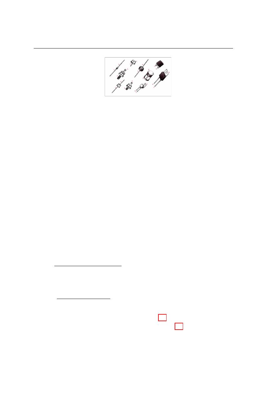
64
Diodes and their applications
Figure 4.1: Typical diode packages with terminal identification.
• Majority carriers flow toward the (pn) junction.
• Majority carriers provide the forward Current.
• The depletion region narrows.
Reverse bias:
• Bias voltage connections: positive to (n) region; negative to (p) region.
• The bias voltage must be less than the breakdown voltage.
• Majority carriers flow away from the (pn) junction during short transition time.
• Minority carriers provide the extremely small reverse current.
• There is no majority carrier current after transition time.
• The depletion region widens.
4.2
The diode model
There are three models of the diode:
4.2.1
The ideal model
The ideal model of a diode is a simple switch. When the diode is forward biased,
it acts like closed (on) switch, as shown in figure 4.2a. When the diode is reversed
biased. It acts like an open (of f ) switch, as shown figure 4.2b. The barrier potential,
the forward dynamic resistance, and the reverse current are all neglected.
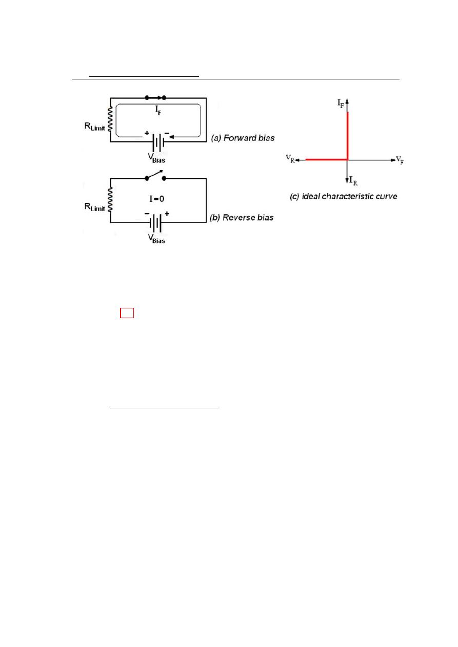
4.2
The diode model
65
Figure 4.2: The ideal model of the diode (a) forward bias, (b) reverse bias and (c) ideal
characteristic curve.
In figure 4.2c, the ideal V − I characteristic curve graphically depicts the ideal diode
operation.
In the ideal diode model: V
F
= 0, I
R
= 0 and V
R
= V
bias
.
4.2.2
The practical model
The practical model adds the barrier potential to the ideal switch model. When
the diode is forward biased, it is equivalent to a closed switch in series with a small
equivalent voltage source equal to the barrier potential with the positive side toward
the anode, as indicated in figure3a. This equivalent voltage source represents the fixed
voltage drop (V
F
) produced across the forward biased (p − n) junction of the diode and
is not an active source of voltage. This voltage (V
F
) consists of the barrier potential
voltage (V
o
) plus the small voltage drop across dynamic resistance of the diode (r
d
), as
indicated by the portion of the curve to the right of the origin. The curve slopes because
the voltage drops due to dynamic (r
d
) as the current increases.
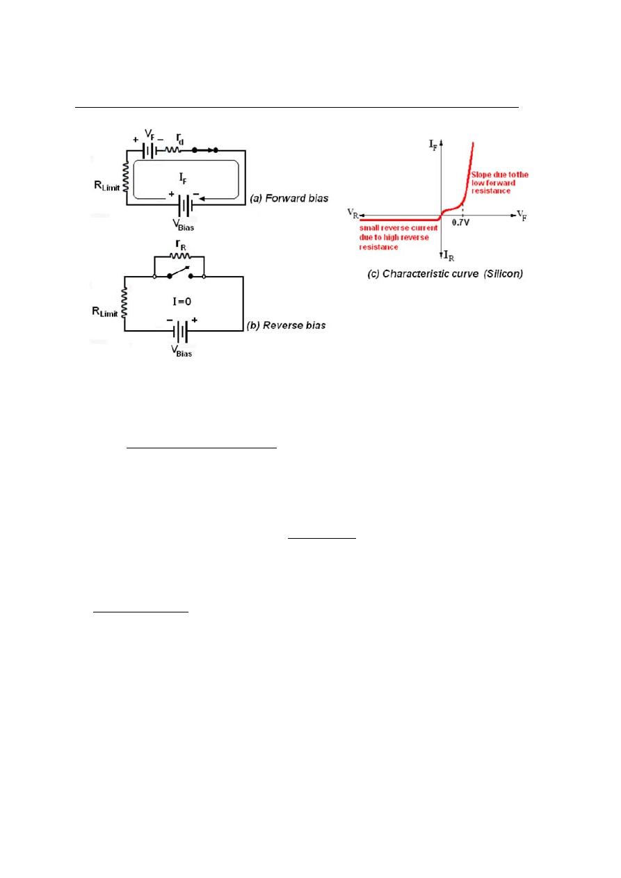
66
Diodes and their applications
Figure 4.3: The complete model of the diode (a) forward bias, (b) reverse bias and (c)
ideal characteristic curve (silicon).
4.2.3
The complete model
For the complete model of a silicon diode, the following formulas apply:
V
F
= V
o
+ I
F
× r
d
I
F
=
(V
Bias
− V
o
)
(R
Limit
+ r
d
)
The reverse current is taken into account with the parallel resistance and is indicated
by the portion of the curve to the left of the origin.
Solved problem
a) Determine the forward voltage and forward current for the diode in figure (a) for
each of the diode models. Also find the voltage across the limiting resistor in each case.
Assume r
d
= 10Ω at the determined value of forward current.
b) Determine the reverse voltage and reverse current for the diode in figure (b) for
each of the diode models. Also find the voltage across the limiting resistor in each case.
Assume I
R
=1µA.
Solution:
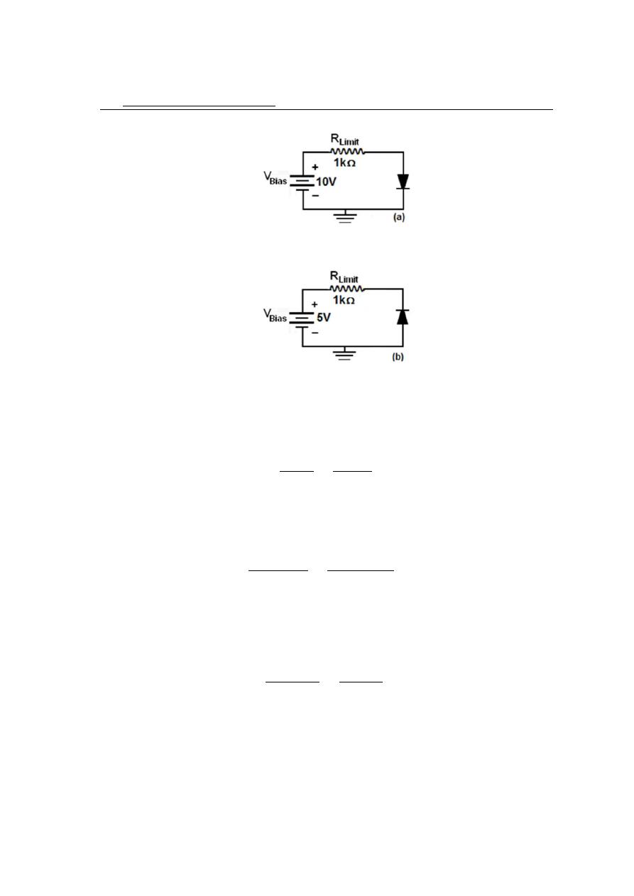
4.2
The diode model
67
Figure 4.4:
Figure 4.5:
a) Ideal model:
V
F
= 0 volt
I
F
=
V
bias
R
Limit
=
10
1 × 10
3
= 10 mA
V
R
limit
= I
F
× R
Limit
= 10 mA × 1kΩ = 10 volt
Practical model:
V
F
= 0.7 volt
I
F
=
V
bias
− V
F
R
Limit
+ r
d
=
10 − 0.7
1 × 10
3
+ 10
= 9.21 mA
V
d
= 0.7 + I
F
× r
d
= 0.7 + 9.21mA × 10 = 792mV
V
R
limit
= I
F
× R
Limit
= 9.21 mA × 1kΩ = 9.21 volt
If we neglected r
d
then;
I
F
=
V
bias
− V
F
R
Limit
=
10 − 0.7
1 × 10
3
= 9.3 mA
V
R
limit
= I
F
× R
Limit
= 9.3 mA × 1kΩ = 9.3 volt
b) Ideal model:
I
R
= 0 A
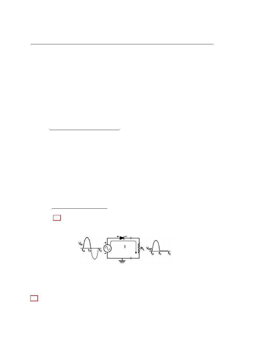
68
Diodes and their applications
V
R
= V Bias = 5 V
V
R
limit
= 0 volt
Practical model
I
R
= 1 µA
V
R(limit)
= I
R
× R
(
Limit) = 1µA × 1kΩ = 1mV
V
R
= V
(
Bias) − V
R
(
limit)=5V −1mV =4.999 volt
4.3
Diode Applications
Because of their ability to conduct current in one direction and block current in the
other direction, diodes are used in circuits called rectifiers that convert ac voltage into
dc voltage. Rectifiers are found in all dc power supplies that operate from an ac voltage
source. A power supply is an essential part of each electronic system from the simplest
to the most complex. In this section, you will study the most basic type of rectifiers,
the half-wave rectifier, full-wave rectifiers and power supply filters and regulators, and
the diode limiting and clamping circuits, and voltage multipliers.
4.3.1
Half-wave rectifier
Figure 4.6, illustrates the process called half wave rectification. The diode connection
to an ac source and to a load resistor R
L
will form a half-wave rectifier. When the input
Figure 4.6: Half-wave rectifier circuit with the input and output voltage waveform.
voltage (V
i
n) goes positive during the time duration between t
0
to t
1
, as shown in Figure
4.6, the diode will biased forward and conducts current through the load resistor. The
current produces an output voltage across the load R
L
which has the same shape as
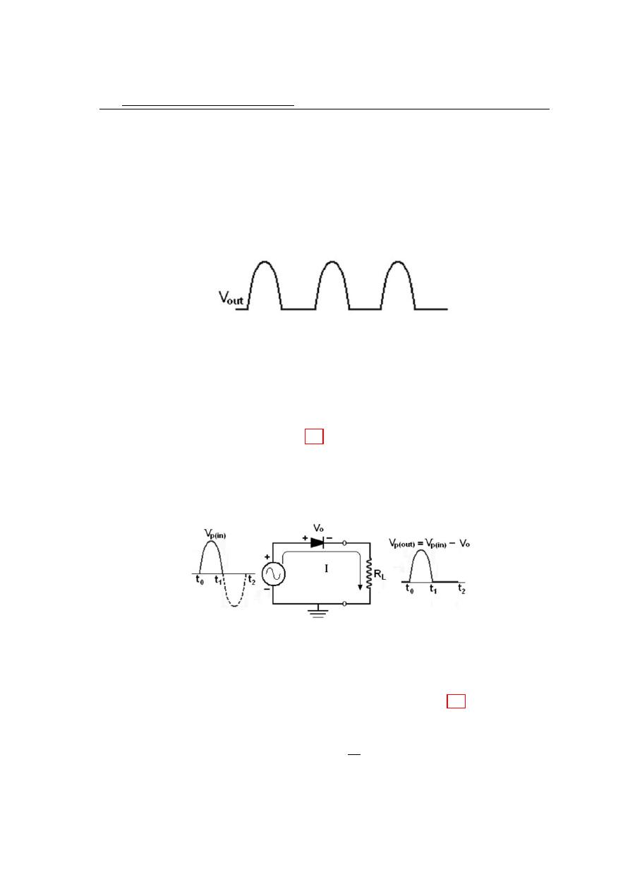
4.3
Diode Applications
69
the positive half cycle of the input voltage. As the input voltage goes negative, during
the second half of the input voltage cycle (t
1
to t
2
), the diode will biased reverse. As
a result there is no current will pass through the load R
L
and the voltage across the
load resistor is 0 V . The net result is that only the positive half cycles of the ac input
voltage appear across the load as shown in Figure 5. Since the output does not change
polarity, it is a pulse dc voltage. When the practical diode model is used with the
Figure 4.7: Half-wave output voltage for three input cycles.
barrier potential of (V
o
) taken into account. During the positive half cycle, the input
voltage must overcome the barrier potential before the diode becomes forward biased.
This result in a half wave output with a peak value that is less than the peak value of
the input by (V
o
), as shown in Figure 4.8.
V
p(out)
= V
p(in)
− V
o
The mean value of the output voltage (V
avg
or V
dc
) can be calculated mathematically
Figure 4.8: The effect of the barrier potential on the half wave rectified output voltage
is to reduce the peak value of the input by V
o
.
by the area under the curve over a full cycle, as shown in Figure 4.9 dividing by 2π, the
number of radians in a full cycle, where V
p
is the peak value of the voltage.
V
avg
=
V
p
π
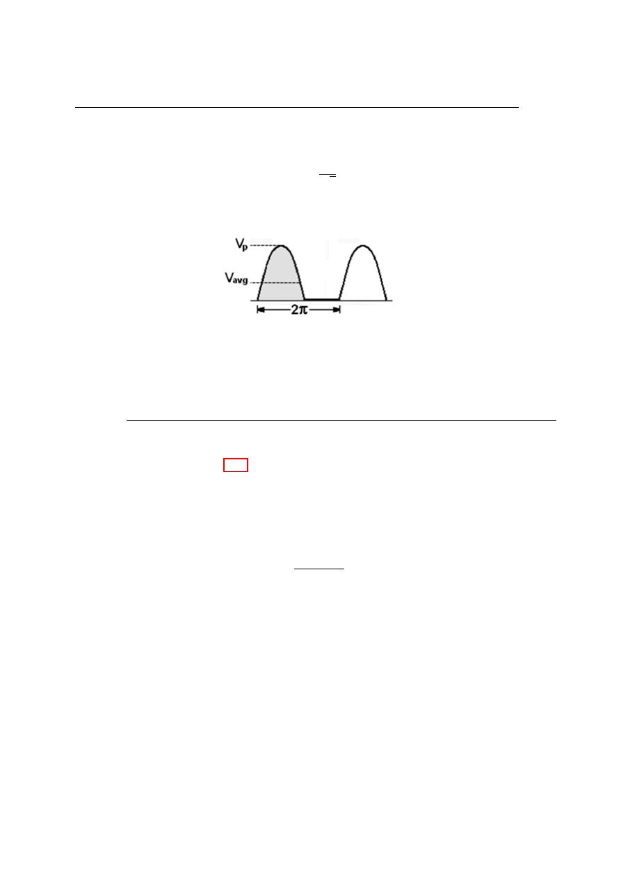
70
Diodes and their applications
The root mean square value of the output voltage (V
rms
) is given as:
V
rms
=
V
p
√
2
Figure 4.9: Average value of the half wave rectified signal.
4.3.5
Half wave rectifier with transformer coupled input voltage
A transformer is often used to couple the ac input voltage from the source to the
rectifier, as shown in figure 4.10. Transformer coupling provides two advantages: 1. It
allows the source voltage to be stepped up or stepped down as needed. 2. The ac source
is electrically isolated from the rectifier, thus preventing a shock hazard in the secondary
circuit. The turn’s ratio (n) is equal to the ratio of secondary turns (N
secondary
) to the
primary turns (N
primary
):
n =
N
secondary
N
primary
N
secondary
= n × N
primary
If n > 1, the secondary voltage is greater than the primary voltage. If n < 1, the sec-
ondary voltage is less than the primary voltage. The peak secondary voltage, V
p(secondary)
in a transformer coupled half wave rectifier is equal to V p(in). Therefore:
V
p(out)
= V
p(secondary)
− V
o
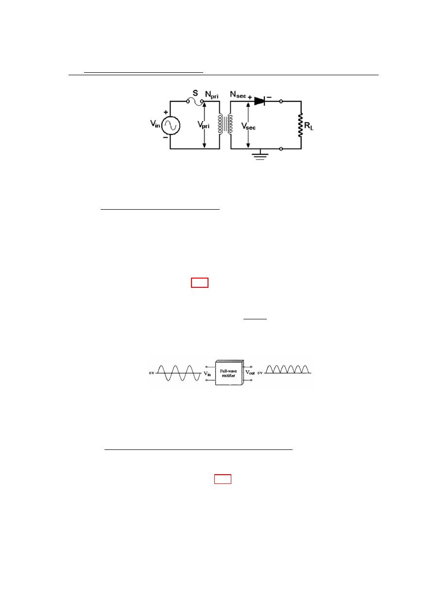
4.4
Full Wave Rectifier
71
Figure 4.10: Half wave rectifier with transformer coupled input voltage.
4.4
Full Wave Rectifier
A full-wave rectifier allows unidirectional (one-way) current through the load during
the entire 360
o
of the input cycle, whereas a half-wave rectifier allow current through
the load only during one-half of the cycle. The result of full-wave rectification is an
output voltage with a frequency twice the input frequency that pulsate every half-cycle
of the input, as shown in Figure 4.11. The average or dc value for a full wave rectified
sinusoidal voltage is twice that of the half wave, as shown in the following formula:
V
dc
= V
avg
=
2 × V
p
π
V
a
vg is approximately 63.7% of V
P
for a full wave rectifiered voltage.
Figure 4.11: Full wave rectifier.
4.6.1
The centre tapped full wave rectifier
A centre tapped rectifier use two diodes connected to the secondary of a center
tapped transformer as shown in figure 4.12. The input voltage is coupled through the
transformer to the centre tapped secondary. Half of the total secondary voltage appears
between the center tap and each end of the secondary winding as shown. For a positive
half cycle of the input voltage, the polarities of the secondary voltages are as shown in
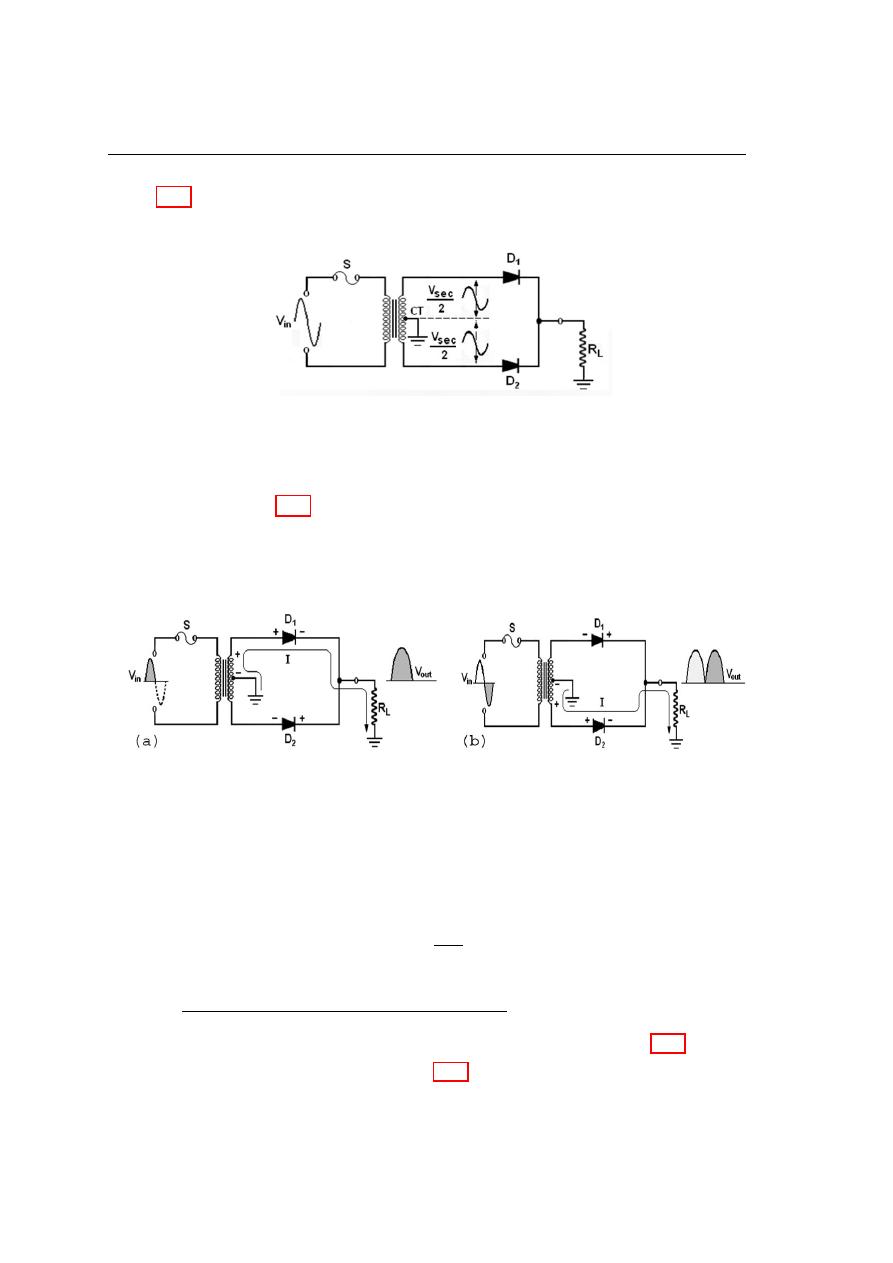
72
Diodes and their applications
figure 4.13(a). This condition forward biases diode D
1
and reverse biases diode D
2
.
The current path is through D
1
and the load resistor R
L
as indicated.
Figure 4.12: A centre-tapped full-wave rectifier.
For a negative half cycle of the input voltage, the voltage polarities on the secondary
are as shown in figure 4.13(b). This condition reverses biases D
1
and forward biases D
2
.
The current path is through D
2
and R
L
as indicated. Because the output current during
through the load, the output voltage developed across the load resistor is a full wave
rectified dc voltage as shown. The output voltage of a center tapped full wave rectifier
Figure 4.13: Basic operation of a centre tapped full wave rectifier. a) During positive
half cycles, D
1
is forward biased and D
2
is reverse biased. b) During negative half cycles.
D
2
is forward-biased and D
1
is reverse biased.
is always one half of the total secondary voltage less the diode drop, no matter what
is the turn’s ratio.
V
out
=
V
sec
2
− V
o
4.6.8
The Bridge Full wave Rectifier
The bridge rectifier uses four diodes connected as shown in figure 4.14. When the
input cycle is positive, as shown in figure 4.14a, diodes D
1
and D
2
are forward biased
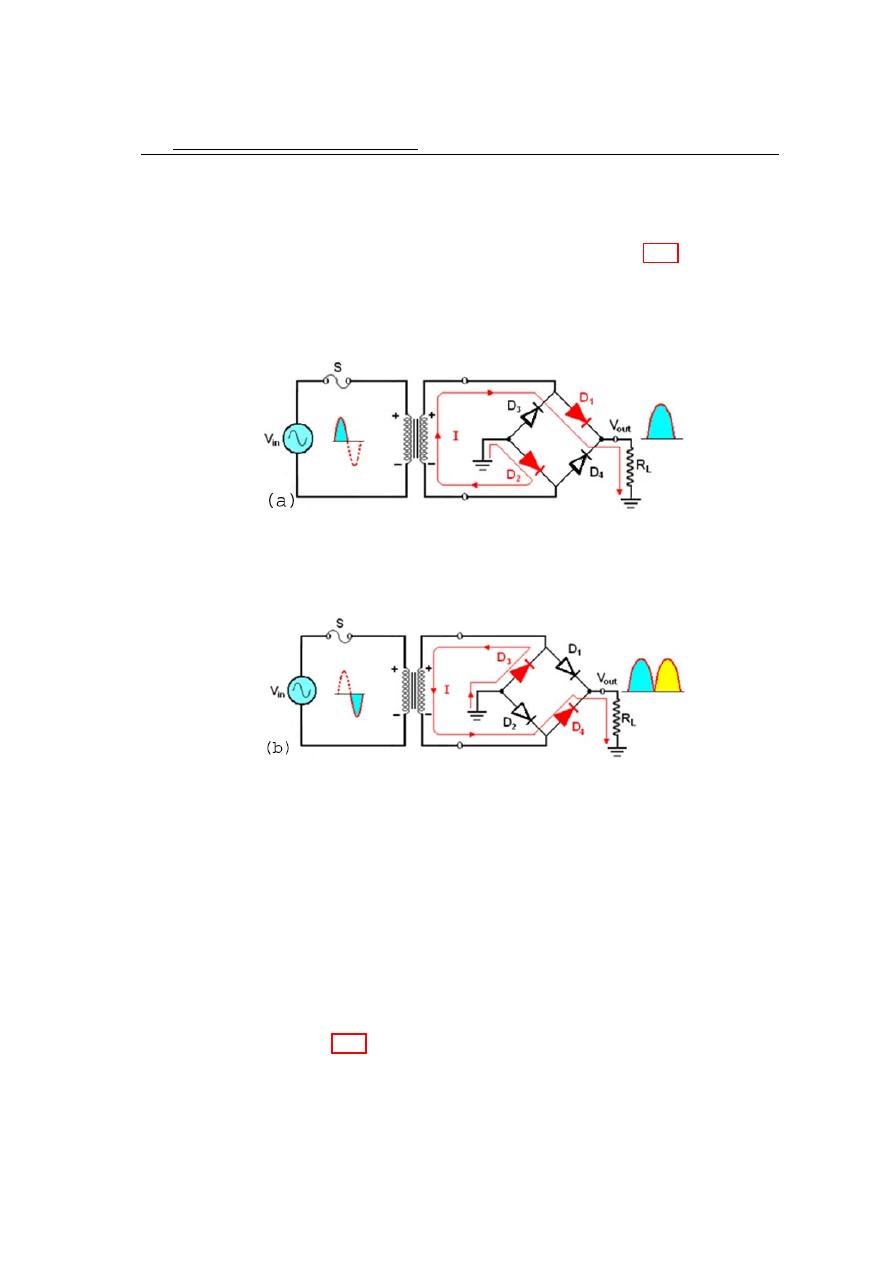
4.4
Full Wave Rectifier
73
and conduct current in the direction shown by arrow. A voltage is developed across R
L
that looks like the positive half of the input cycle. During this time, diodes D
3
and D
4
are reverse biased. When the input cycle is negative as in figure 4.15b, diodes D
3
and
D
4
are forward biased and conduct current in the same direction through R
L
as during
the positive half cycle. During the negative half cycle, D
1
and D
2
are reverse biased. A
full wave rectified output voltage appears across R
L
as a result of this action. Bridge
Figure 4.14: Figure 12(a) During the positive half cycle of the input. D
1
and D
2
are
forward biased and conduct current D
3
and D
4
are reverse biased.
Figure 4.15: Figure 12(b) During the negative half cycle of the input. D
3
and D
4
are
forward biased and conduct current while D
1
and D
2
are reverse biased.
output voltage:
During the positive half cycle of the total secondary voltage, diodes D
1
and D
2
are
forward biased. Neglecting the diode drops, the secondary voltage appears across the
load resistor. The same is true when D
3
and D
4
are forward biased during the negative
half cycle.
V
p(out)
= V
p(sec)
It can be seen in figure 4.16. Two diodes are always in series with the load resistor
during both the positive and negative half cycles. If these diode drops are taken into
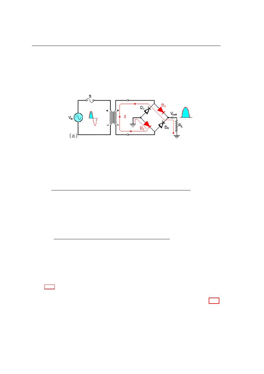
74
Diodes and their applications
account, the output voltage is:
V
p(out)
= V
p(sec)
− V
o
Figure 4.16: Bridge operation during a positive half cycle of the primary and secondary
voltages.
4.7
Power Supply Filters and Regulators
In the most power supply applications, the standard 50 Hz AC power line voltage
should be converted to an approximately constant DC voltage. The pulsating DC output
of a rectifier must be filtered to reduce the large voltage variations.
4.9.1
Power Supply Filters and Regulators
The filter is simply a capacitor connected from the rectifier output to ground. R
L
represents the equivalent resistance of a load.
1. During the positive first quarter cycle of the input, the diode is forward biased,
allowing the capacitor to charge to within V
o
of the input peak, as shown in figure
2. When the input begins to decrease below its peak. As shown in figure 4.18, the
capacitor retains its charge and the diode becomes reverse biased because the
cathode is more positive than the anode. During the remaining part of the cycle,
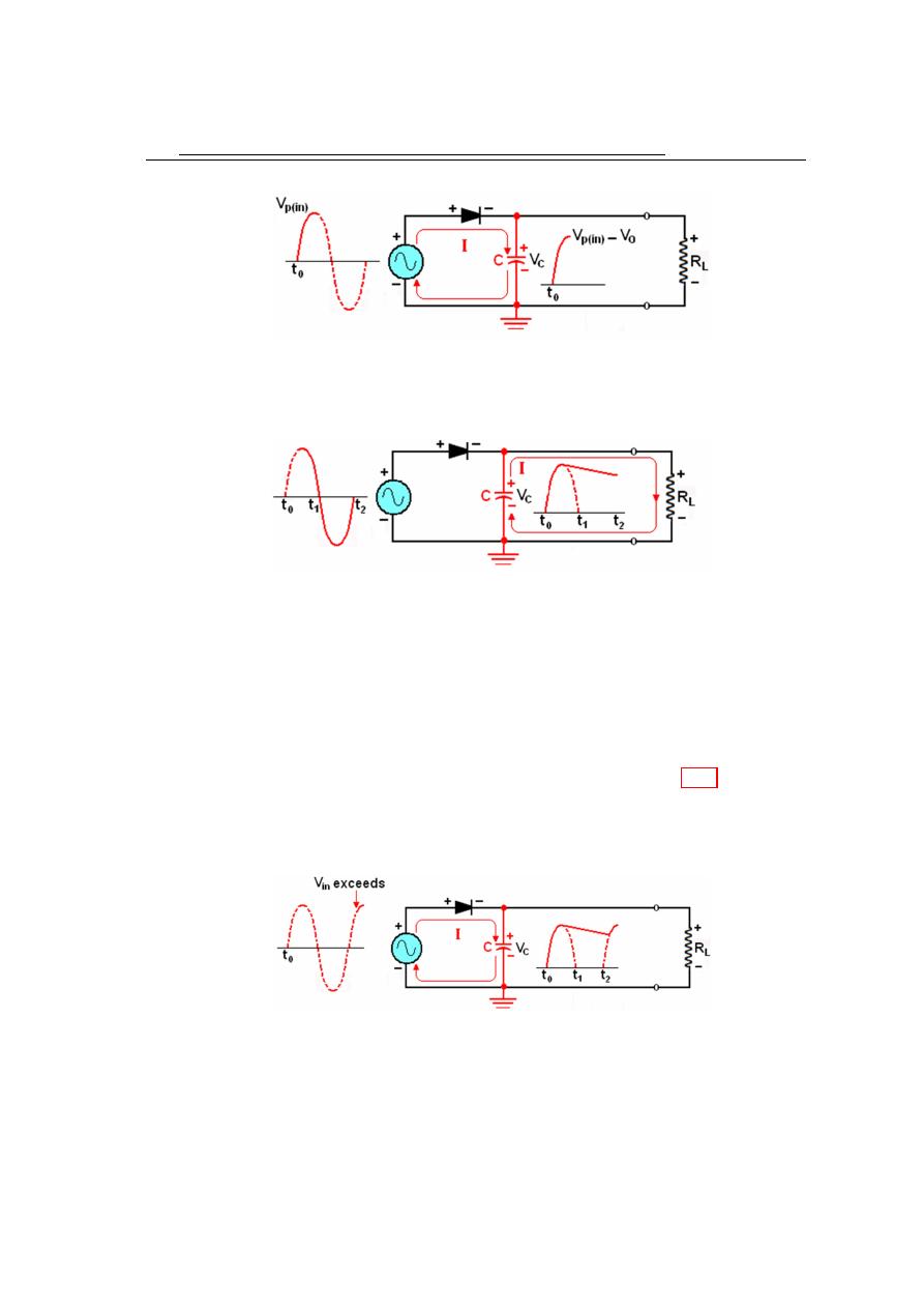
4.7
Power Supply Filters and Regulators
75
Figure 4.17: Initial charging of the capacitor (diode is forward biased) happens only
once when power is turned on.
Figure 4.18: The capacitor discharges through R
L
after peak of positive alternation
when the diode is reverse biased.
the capacitor can discharge only through the load resistance at a rate determined
by the R
L
C time constant.
3. During the first quarter of the next cycle, as shown in figure 4.19, the diode will
again become forward biased when the input voltage exceeds the capacitor voltage
by approximately V
o
.
Figure 4.19: The capacitor charges back to peak of input when the diode becomes
forward-biased.
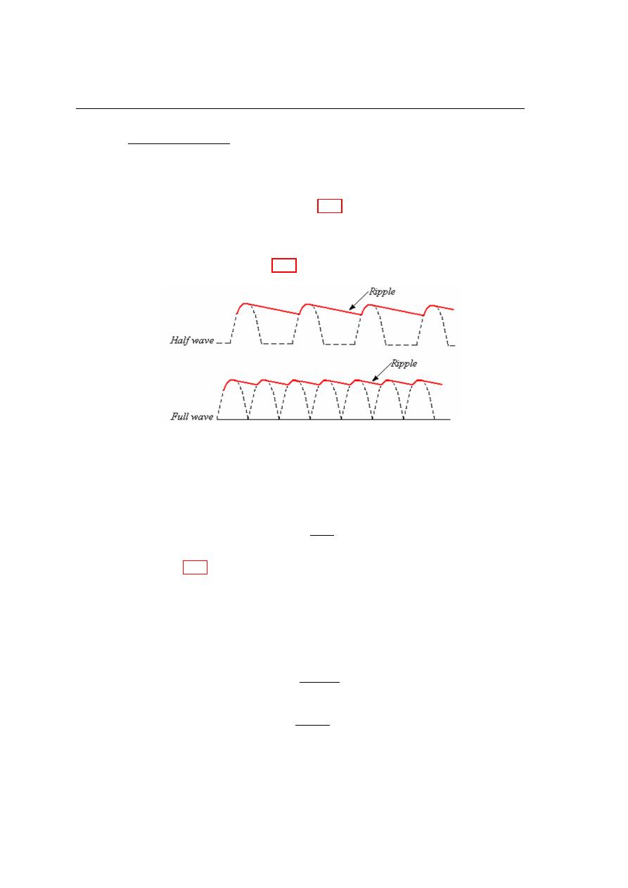
76
Diodes and their applications
4.9.2
Ripple Factor
The variation in the capacitor voltage due to the charging and discharging is called
the ripple voltage. Generally, ripple is undesirable; thus, the smaller the ripple, the
better the filtering action, as shown in figure 4.20. When filtered, the full wave rectified
voltage has a smaller ripple than does a half wave voltage for the same load resistance
and capacitor values. The capacitor discharges less during the shorter interval between
full-wave pulses, as shown in figure 4.20a and b. The ripple factor is an indication of
Figure 4.20: Comparison of ripple voltages for (a) half wave and (b) full wave rectified
voltages with the same filter capacitor and load.
the effectiveness of the filter and is defined as:
r =
V
rms
V
dc
As shown in figure 4.21. The ripple factor can be lowered by increasing the value of
the filter capacitor or increasing the load resistance. For a full wave rectifier with a
capacitor input filter, approximations for the peak to peak ripple voltage, V
rms
and the
DC value of the filter output voltage is V
d.c
, are given in the following expressions. The
variable V
p(rect)
is the unfiltered peak rectified voltage.
V
dc
=
1 −
0.00417
R
L
C
V
p(rect)
V
rms
=
0.0024
R
L
C
V
p(rect)
The last formulas are for ripple filtered signal.
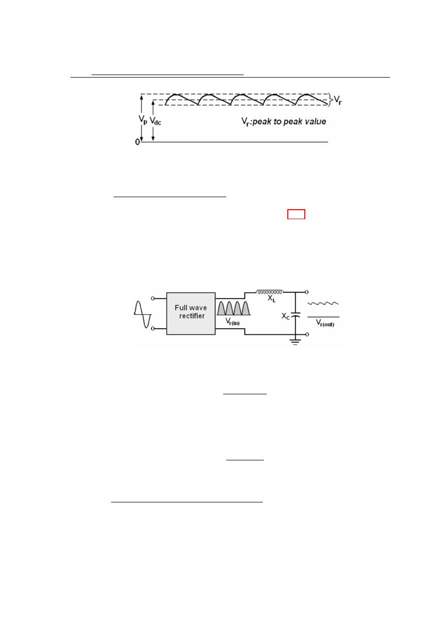
4.12
Diode Clipping Circuits
77
Figure 4.21: V
rms
and V
dc
determination for the ripple factor calculation
4.10.3
Inductor Input Filter
When a choke is add to the filter input, as in figure 4.22, a reduction in the ripple
voltage V
rms
is achieved. The choke has a high reactance at the ripple frequency. The
capacitive reactance is low compared to both R
L
and X
L
(10 time at least).
The
magnitude of the out ripple voltage of the filter is determined with voltage divider
equation:
Figure 4.22: The LC filter as it look to the AC component.
V
rms(out)
=
X
C
|X
L
− X
C
|
V
rms(in)
Since the choke presents a winding resistance R
w
in series with load resistance R
L
.
This resistance produce undesirable reduction of DC value, therefore R
w
must be small
compared of R
L
.
V
dc(out)
=
R
L
R
L
− R
w
V
dc(in)
4.12
Diode Clipping Circuits
Diode circuits, called limiters or clippers, are sometimes used to clip off portions
of signal voltages above or below certain levels. Another type of diode circuit, called
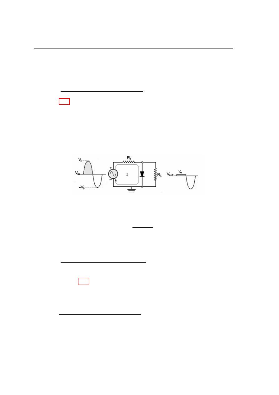
78
Diodes and their applications
a clamper, is used to add or restore a DC level to an electrical signal. In the present
lecture we will discuss the clipping circuits only.
4.12.1
Positive Clipping Circuit
Figure 4.23 shows a diode clipper that clips the positive part of the input voltage.
As the input voltage goes positive, the diode becomes forward biased and conducts the
current. So point A is limited to (+ V
o
), when the input go back below V
o
, the diode is
reverse biased and appears as an open the output voltage is look like the negative part
of the input voltage, but with magnitude determined by the voltage divider formed by
R
1
and the load resistance R
L
, as follow:
Figure 4.23: Circuit for the positive clipper.
V
out
=
R
L
R
L
+ R
1
V
in
if R
1
is much less than R
L
⇒ V
out
≈ V
in
4.13.2
Negative Clipping Circuit
To obtain negative biased clipper circuit, the diode and bias voltage must connect
as shown in figure 4.24. In this case, the voltage at point A must go below (−V
B
− V
o
)
to forward bias the diode an initiate limiting action as shown.
4.15
Voltage Divider Bias
The bias voltage sources that have been used to explain the basic operation of diode
limiter can be replaced by a resistive voltage divider that derives the desired bias voltage
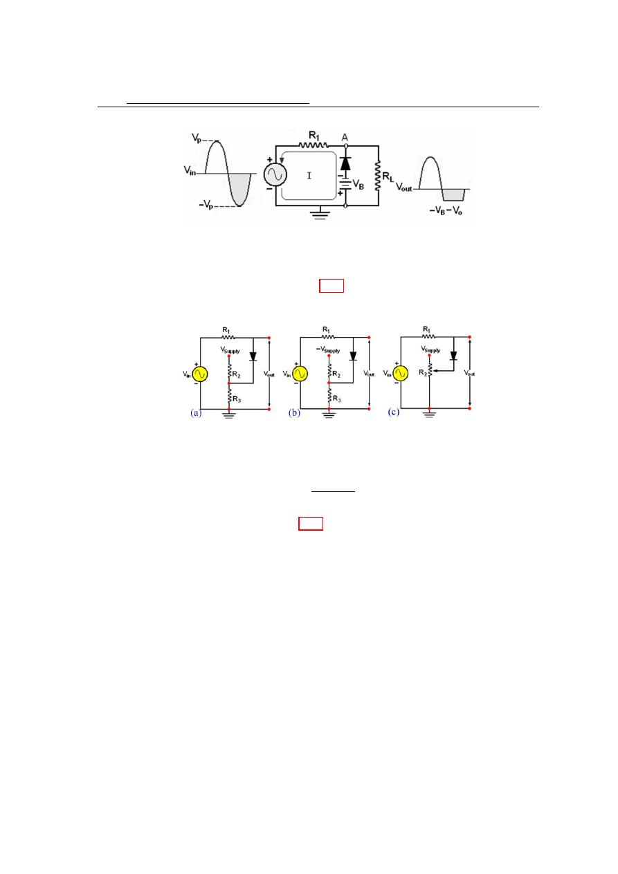
4.15
Voltage Divider Bias
79
Figure 4.24: Circuit for the negative clipper.
from the dc supply voltage, as shown in 4.25. The bias voltage is set by the resistor
values according to the voltage divider formula.
Figure 4.25: Circuit for the negative clipper.
V
Bias
=
R
3
R
2
+ R
3
V
supply
A positively biased limiter is shown in 4.25a, a negatively biased limiter is shown in part
(b), and a variable positive bias circuit using a potentiometer voltage divider is shown in
part (c). The bias resistors must be small compared to (R), so that the forward current
through the diode will not affect the bias voltage.