
Instructor's Solution Manual with Transparency Masters
THE 8088 AND 8086 MICROPROCESSORS
Programming, Interfacing,
Software, Hardware,
and Applications
Fourth Edition
Walter A. Triebel
Fairliegh Dickinson University
Avtar Singh
San Jose State University
Including the 80286, 80386, 80486, and Pentium
TM
Processors

CONTENTS
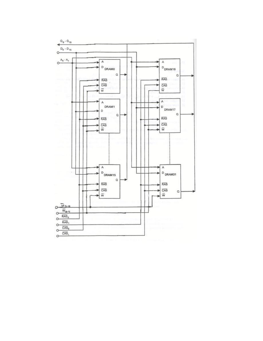
Chapter
Page
1
Introduction to Microprocessors and Microcomputers
4
2
Software Architecture of the 8088 and 8086 Microprocessors
5
3 Assembly Language Programming
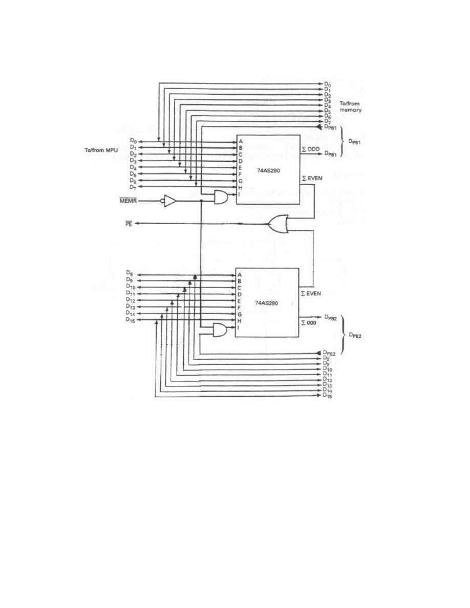
9
4
Machine Language Coding and the DEBUG Software Development
11
Program of the PC
5 8088/8086 Programming —Integer Instructions and Computations
16
6 8088/8086 Programming —Control Flow Instructions and Program
23
Structures
7 Assembly Language Program Development with MASM
33
8
The 8088 and 8086 Microprocessors and their Memo ry
35
and Input/Output Interfaces
9
Memory Devices, Circuits, and Subsystem Design
42
10 Input/Output Interface Circuits and LSI Peripheral Devices
49
11 Interrupt Interface of the 8088 and 8086 Microprocessors
55
12 Hardware of the Original IBM PC Microcomputer
58
13 PC Bus Interfacing, Circuit Construction, Testing, and
63
Troubleshooting
14 Real-Mode Software and Hardware Architecture of the 80286
68
Microprocessor
15 The 80386, 80486, and Pentium
R
Processor Families: Software
71
Architecture
16 The 80386, 80486, and Pentium
R
Processor Families: Hardware
77
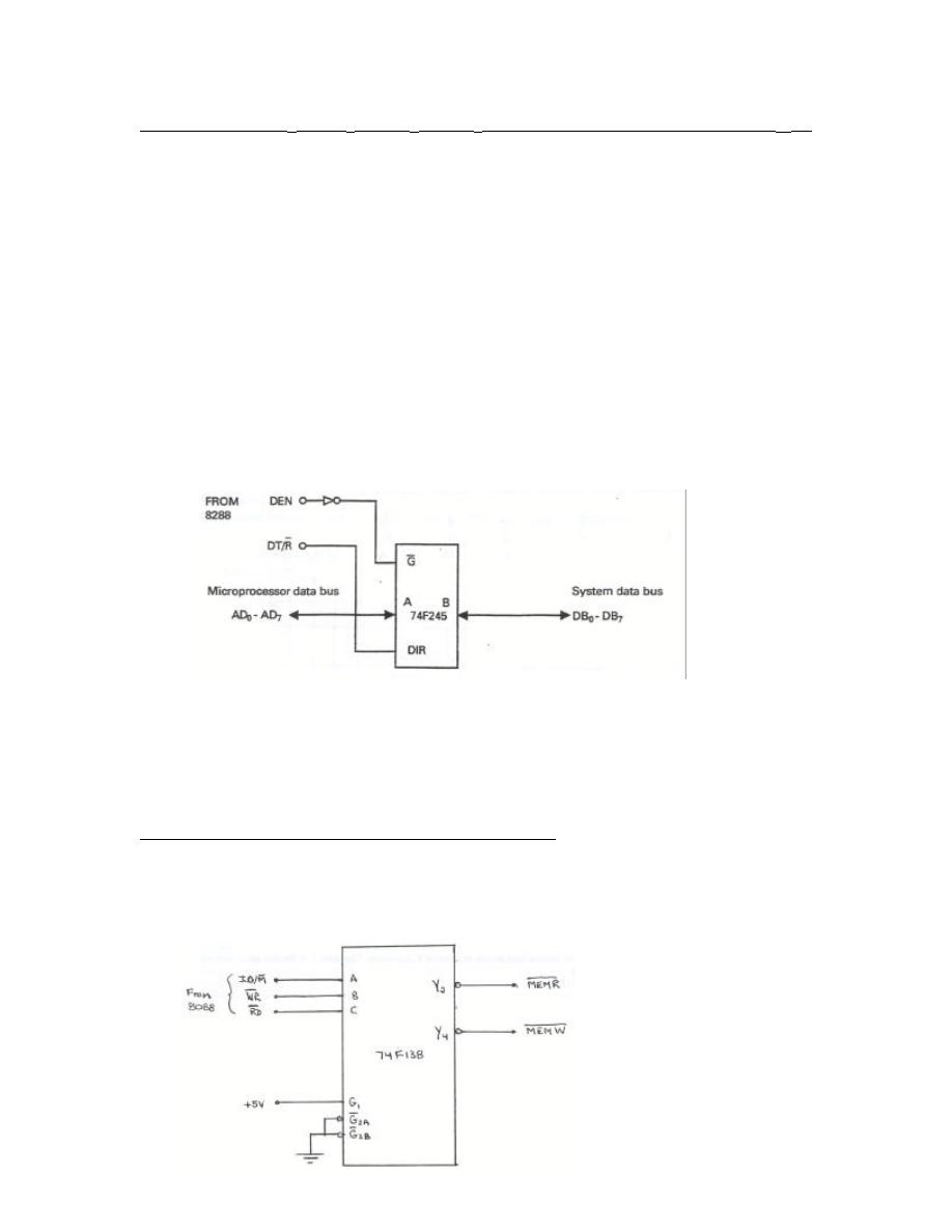
Architecture

PREFACE
This manual contains solutions or answers to the assignment problems at the end of each
chapter.
Another supplements available from Prentice-Hall for the textbook is:
Laboratory Manual: ISBN: 0-13-045231-9
Laboratory Manual to Accompany
The 8088 and 8086 Microprocessors:
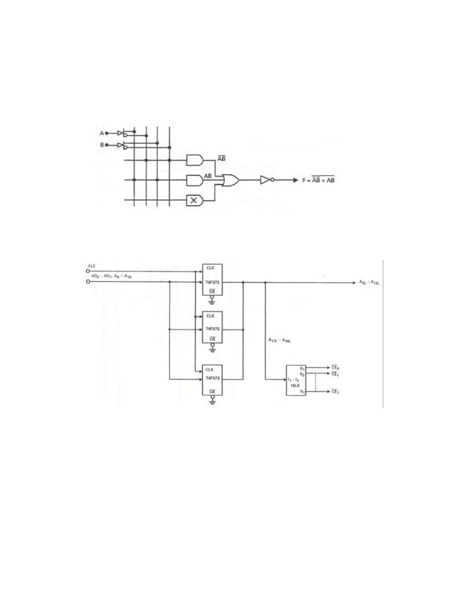
Programming, Interfacing, Software,
Hardware, and Applications, Fourth Edition
Walter A. Triebel and Avtar Singh
c. 2003
Pearson Education, Inc.
Support products available from third parties are as follows:
Microsoft Macroassembler
Microsoft Corporation, Redmond, WA 98052
800-426-9400
PC
µ
LAB- Laboratory Interface Circuit Test Unit
Microcomputer Directions, Inc.
P.O. Box 15127, Fremont, CA 94539
973-872-9082

CHAPTER 1
Section 1.1
1.
Original IBM PC.
2.
A system whose functionality expands by simply adding special function boards.
3.
I/O channel.
4.
Personal computer advanced technology.
5.
Industry standard architecture.
6.
Peripheral component interface (PCI) bus
7.
A reprogrammable microcomputer is a general-purpose computer designed to run
programs for a wide variety of applications, for instance, accounting, word processing,
and languages such as BASIC.
8.
Mainframe computer, minicomputer, and microcomputer.
9.
The microcomputer is similar to the minicomputer in that it is designed to perform
general-purpose data processing; however, it is smaller in size, has reduced capabilities,
and cost less than a minicomputer.
10.
Very large scale integration.
Section 1.2
11.
Input unit, output unit, microprocessing unit, and memory unit.
12.
Microprocessing unit (MPU).
13.
16-bit.
14.
Keyboard; mouse and scanner.
15.
Monitor and printer.
16.
Primary storage and secondary storage memory.
17.
360K bytes; 10M bytes.
18.
Read-only memory (ROM) and random access read/write memory (RAM).
19.
48K bytes; 256K bytes.
20.
The Windows98
R
program is loaded from the hard disk into RAM and then run. Since
RAM is volatile, the operating system is lost whenever power is turned off.
Section 1.3
21.
4-bit, 8-bit, 16-bit, 32-bit, and 64-bit.
22.
4004, 8008, 8086, 80386DX.
23.
8086, 8088, 80186, 80188, 80286.
24.
Million instructions per second.
25.
27 MIPS
26.
Drystone program.
27.
39; 49.
28.
30,000, 140,000, 275,000, 1,200,000, 3,000,000.
29.
A special purpose microcomputer that performs a dedicated control function.
30.
Event controller and data controller.

31.
A multichip microcomputer is constructed from separate MPU, memory, and I/O
ICs. On the other hand, in a single chip microcomputer, the MPU, memory, and I/O
functions are all integrated into one IC.
32.
8088, 8086, 80286, 80386DX, 80486DX, and Pentium
R
processor.
33.
Real mode and protected mode.
34.
Upward software compatible means that programs written for the 8088 or 8086 will
run directly on the 80286, 80386DX, and 80486DX.
35.
Memory management, protection, and multitasking.
36.
Floppy disk controller, communication controller, and local area network controller.
Section 1.4
37.
MSB and LSB.
38.
2
-2
= 1/4
39.
1 and 2
+5
= 16
10
; 1 and 2
-4
= 1/16
40.
(a) 6
10
, (b) 21
10
, (c) 127
10
.
41.
Min = 00000000
2
= 0
10
, Max = 11111111
2
= 255
10
.
42.
(a) 00001001
2
, (b) 00101010
2
, (c) 01100100
2
43.
0000000111110100
2
44.
(a) .1
2
(b) .01
2
(c) .01011
2
45.
C and 16
+2
= 256
10
46.
16
+4
= 65,536
10
47.
(a) 39H, (b) E2H, (c) 03A0H.
48.
(a) 01101011
2
, (b) 11110011
2
, (c) 0000001010110000
2
.
49.
C6H, 198
10
.
50.
MSB = 1, LSB = 0.
51.
8005AH, 1,048,666
10
.
CHAPTER 2
Section 2.1
1.
Bus interface unit and execution unit.
2.
BIU.
3.
20 bits; 16 bits.
4.
4 bytes; 6 bytes.
5.
General-purpose registers, temporary operand registers, arithmetic logic unit (ALU),
and status and control flags.
Section 2.2
6.
Aid to the assembly language programmer for understanding a microprocessor's
software operation.
7.
There purpose, function, operating capabilities, and limitations.
8.
14
9.
1,048,576 (1M) bytes.

10.
65,536 (64K) bytes.
Section 2.3
11.
FFFFF
16
and 00000
16
.
12.
Bytes.
13.
00FF
16
; aligned word.
14.
44332211
16
; misaligned double word.
15.
Address Contents
0A003H CDH
0A004H ABH
aligned word.
16.
Address Contents
0A001H 78H
0A002H 56H
0A003H 34H
0A004H 12H
misaligned double word.
Section 2.4
17.
Unsigned integer, signed integer, unpacked BCD, packed BCD, and ASCII.
18.
(a) 7FH
(b) F6H
(c) 80H
(d) 01F4H
19.
(0A000H) = F4H
(0A001H) = 01H
20.
-1000 = 2's complement of 1000
= FC18H
21.
(a) 00000010, 00001001; 00101001
(b) 00001000, 00001000; 10001000
22.
(0B000H) = 09H
(0B001H) = 02H
23.
NEXT I
24.
(0C000H) = 34H
(0C001H) = 33H
(0C002H) = 32H
(0C003H) = 31H
Section 2.5
25.
64Kbytes.
26.
Code segment (CS) register, stack segment (SS) register, data segment (DS) register,
and extra segment (ES) register.
27.
CS.

28.
Up to 256Kbytes.
29.
Up to 128Kbytes.
Section 2.6
30.
Pointers to interrupt service routines.
31.
80
16
through FFFEF
16
.
32.
Instructions of the program can be stored anywhere in the general -use part of the
memory address space.
33.
Control transfer to the reset power-up initialization software routine.
Section 2.7
34.
The instruction pointer is the offset address of the next instruction to be fetched by
the 8088 relative to the current value in CS.
35.
The instruction is fetched from memory; decoded within the 8088; op erands are read
from memory or internal registers; the operation specified by the instruction is performed
on the data; and results are written back to either memory or an internal register.
36.
IP is incremented such that it points to the next sequenti al word of instruction code.
Section 2.8
37.
Accumulator (A) register, base (B) register, count (C) register, and data (D) register.
38.
With a postscript X to form AX, BX, CX, and DX.
39.
DH and DL.
40.
Count for string operations and count for loop ope rations.
Section 2.9
41.
Offset address of a memory location relative to a segment base address.
42.
Base pointer (BP) and stack pointer (SP).
43.
SS
44.
DS
45
. Source index register; destination index register.
46.
The address in SI is the o ffset to a source operand and DI contains the offset to a
destination operand.
Section 2.10
47.
Flag Type
CF Status
PF Status
AF Status
ZF Status
SF Status
OF Status

TF Control
IF Control
DF Control
48.
CF = 1, if a carry-out/borrow-in results for the MSB during the execution of an
arithmetic instruction. Else it is 0.
PF = 1, if the result produced by execution of an instruction has even parity. Else it is 0.
AF = 1, if there is a carry-out/borrow-in for the fourth bit during the execution of an
arithmetic instruction.
ZF = 1, if the result produced by execution of an instruction is zero. Else it is 0.
SF = 1, if the result produced by execution o f an instruction is negative. Else it is 0.
OF = 1, if an overflow condition occurs during the execution of an arithmetic instruction.
Else it is 0.
49.
Instructions can be used to test the state of these flags and, based on their setting,
modify the sequence in which instructions of the program are executed.
50.
Trap flag
51.
DF
52.
Instructions are provided that can load the complete register or modify specific flag
bits.
Section 2.11
53.
20 bits.
54.
Offset and segment base.
55.
(a) 11234H
(b) 0BBCDH
(c) A32CFH
(d) C2612H
56. (a)
? = 0123H
(b) ? = 2210H
(c) ? = 3570H
(d) ? = 2600H
57.
021AC
16
58.
A000
16
59.
1234
16
Section 2.12
60.
The stack is the area of memory used to temporarily store informat ion (parameters) to
be passed to subroutines and other information such as the contents of IP and CS that is
needed to return from a called subroutine to the main part of the program.
61.
CFF00
16
62.
128 words.
63.
FEFEH
→
(SP)
(AH) = EEH
→
(CFEFFH)
(AL) = 11H
→
(CFEFEH)

Section 2.13
64.
Separate.
65.
64-Kbytes.
66.
Page 0.
CHAPTER 3
Section 3.1
1.
Software.
2.
Program.
3.
Operating system.
4.
80386DX machine code.
5.
Instructions encoded in machine language are coded in 0s and 1s, whi le assembly
language instructions are written with alphanumeric symbols such as MOV, ADD, or
SUB.
6.
Mnemonic that identifies the operation to be performed by the instruction; ADD and
MOV.
7.
The data that is to be processed during execution of an ins truction; source operand and
destination operand.
8.
START; ;Add BX to AX
9.
An assembler is a program that is used to convert an assembly language source
program to its equivalent program in machine code. A compiler is a program that
converts a program written in a high -level language to equivalent machine code.
10.
Programs written is assembly language or high level language statements are called
source code. The machine code output of an assembler or compiler is called object code.
11.
It takes up less memory and executes faster.
12.
A real-time application is one in which the tasks required by the application must be
completed before any other input to the program occurs that can alter its operation.
13.
Floppy disk subsystem control and communicat ions to a printer; code translation and
table sort routines.
Section 3.2
14.
Application specification.
15.
Algorithm; software specification.
16.
A flowchart is a pictorial representation that outlines the software solution to a
problem.
17.

18.
Editor.
19.
Assembler.
20.
Macroassembler.
21.
Linker.
22.
(a)
Creating a source program
(b)
Assembling a source program into an object module
(c)
Producing a run module
(d)
Verifying/debugging a solution
23.
(a)
PROG_A.ASM
(b)
PROG_A.LST and PROG_A.OBJ
(c)
PROG_A.EXE and PROG_A.MAP
Section 3.3
24.
117.
25.
Data transfer instructions, arithmetic instructions, logic instructions, string
manipulation instructions, control transfer instructions, and processor control
instructions.
Section 3.4
26.
Execution of the move instruction transfers a byte or a word of data from a source
location to a destination location.
Section 3.5
27.
An addressing mode means the method by which an operand can be specified in a
register or a memory location.
28.
Register operand addressing mode
Immediate operand addressing mode
Memory operand addressing modes
29.
Base, index, and displacement.
30.
Direct addressing mode
Register indirect addressing mode
Based addressing mode
Indexed addressing mode
Based-indexed addressing mode
31.
Instruction Destination
Source
(a)
Register
Register
(b)
Register
Immediate
(c)
Register indirect
Register
(d)
Register Register indirect

(e)
Based
Register
(f)
Indexed
Register
(g)
Based-indexed
Register
32.
(a)
PA = 0B200
16
(b)
PA = 0B100
16
(c)
PA = 0B700
16
(d)
PA = 0B600
16
(e)
PA = 0B900
16
CHAPTER 4
Section 4.1
1.
6 bytes.
2.
0000001111000010
2
= 03C2H
3.
(a) 1000100100010101
2
= 8915H; (b) 1000100100011000
2
= 8918H;
(c) 100010100101011100010000
2
= 8A5710H
4.
(a) 000111102 = 1EH; (b) 11010010110000112 = D2C3H;
(c)
110000011000110100000100102 = 03063412H
Section 4.2
5.
3 bytes.
6.
24 bytes.
Section 4.3
7.
The DEBUG program allows us to enter a program into the PC's memory, execute i t
under control, view its operation, and modify it to fix errors.
8.
Yes.
9.
Error.
10.
-R CX (
↵
)
CX XXXX
:0010 (
↵
)
11.
-R F (
↵
)
NV UP EI PL NZ NA PO NC -PE (
↵
)
12.
-R
(
↵
)
Section 4.4
13.
-D CS:0000 000F
(
↵
)

14.
-E CS:0 (
↵
)
1342:0000 CD. 20. 00. 40. 00. 9A. EE. FE.
1342:0008 1D. F0. F5. 02. A7. 0A. 2E. 03.
(
↵
)
After a byte of data is displayed, the space bar is depressed to display the next byte. The
values displayed may not be those shown but will be identical to those displayed with the
DUMP command.
15.
-E CS:100 FF FF FF FF FF
(
↵
)
16.
-E SS:(SP) 0 ......0 (32 zeros)
(
↵
)
17.
-F CS:100 105 11 (
↵
)
-F CS:106 10B 22 (
↵
)
-F CS:10C 111 33 (
↵
)
-F CS:112 117 44 (
↵
)
-F CS:118 11D 55 (
↵
)
-E CS:105
(
↵
)
CS:0105 XX.FF (
↵
)
-E CS:113
(
↵
)
-CS:0113 XX.FF (
↵
)
-D CS:100 11D (
↵
)
-S CS:100 11D FF (
↵
)
Section 4.5
18.
Input command and output command.
19.
Contents of the byte-wide input port at address 0123
16
is input and displayed on the
screen.
20.
O 124 5A (
↵
)
Section 4.6
21.
The sum and difference of two hexadecimal numbers.
22.
4 digits.
23.
H FA 5A (
↵
)
Section 4.7
24.
-E CS:100 32 0E 34 12
(
↵
)
-U CS:100 103
(
↵
)
1342:100 320E3412 XOR CL,[1234]

-W CS:100 1 50 1
(
↵
)
25.
-L CS:400 1 50 1
(
↵
)
-U CS:400 403
(
↵
)
1342:0400 320E3412 XOR CL,[1234]
-
Section 4.8
26.
-A CS:100
(
↵
)
1342:0100 MOV [DI],DX (
↵
)
1342:0102
(
↵
)
27.
-A CS:200
(
↵
)
1342:0200 ROL BL,CL
(
↵
)
1342:0202
(
↵
)
-U CS:200 201
(
↵
)
1342:0200 D2C3 ROL BL,CL
-
Section 4.9
28.
-L CS:300 1 50 1 (
↵
)
-U CS:300 303 (
↵
)
-R CX
(
↵
)
CX XXXX
:000F
(
↵
)
-E DS:1234 FF (
↵
)
-T =CS:300 (
↵
)
-D DS:1234 1235 (
↵
)
29.
-N A:BLK.EXE (
↵
)
-L CS:200
(
↵
)
-R DS
(
↵
)
DS 1342
:2000
(
↵
)
-F DS:100 10F FF (
↵
)
-F DS:120 12F 00 (
↵
)
-D DS:100 10F (
↵
)
2000:0100 FF FF FF FF FF FF FF FF-FF FF FF FF FF FF FF FF
-D DS:120 12F (
↵
)
2000:0120 00 00 00 00 00 00 00 00-00 00 00 00 00 00 00 00
-R DS
(
↵
)

DS 2000
:1342
(
↵
)
-R
(
↵
)
AX=0000 BX=0000 CX=0000 DX=0000 SP=FFEE BP=0000 SI=0000 DI=0000
DS=1342 ES=1342 SS=1342 CS=1342 IP=0100 NV UP EI PL NZ NA PO NC
1342:0100 8915 MOV
[DI],DX DS:0000=20CD
-U CS:200 217 (
↵
)
1342:0200 B80020 MOV AX,2000
1342:0203 8ED8 MOV DS,AX
1342:0205 BE0001 MOV SI,0100
1342:0208 BF2001 MOV DI,0120
1342:020B B91000 MOV CX,0010
1342:020E 8A24 MOV AH,[SI]
1342:0210 8825 MOV [DI],AH
1342:0212 46 INC SI
1342:0213 47 INC DI
1342:0214 49 DEC CX
1342:0215 75F7 JNZ 020E
1342:0217 90 NOP
-G =CS:200 217 (
↵
)
AX=FF00 BX=0000 CX=0000 DX=0000 SP=FFEE BP=0000 SI=0110 DI=0130
DS=2000 ES=1342 SS=1342 CS=1342 IP=0217 NV UP EI PL ZR NA PE NC
1342:0217 90 NOP
-D DS:100 10F (
↵
)
2000:0100 FF FF FF FF FF FF FF FF-FF FF FF FF FF FF FF FF
-D DS:120 12F (
↵
)
2000:0120 FF FF FF FF FF FF FF FF-FF FF FF FF FF FF FF FF
Section 4.10
30.
A syntax error is an error in the rules of coding the program. On the other hand, an
execution error is an error in the logic of the planned solution for the problem.
31.
Bugs.
32.
Debugging the program.
33.
-N A:BLK.EXE (
↵
)
-L CS:200
(
↵
)
-U CS:200 217 (
↵
)
1342:0200 B80020 MOV AX,2000
1342:0203 8ED8 MOV DS,AX
1342:0205 BE0001 MOV SI,0100
1342:0208 BF2001 MOV DI,0120
1342:020B B91000 MOV CX,0010
1342:020E 8A24 MOV AH,[SI]
1342:0210 8825 MOV [DI],AH
1342:0212 46 INC SI

1342:0213 47 INC DI
1342:0214 49 DEC CX
1342:0215 75F7 JNZ 020E
1342:0217 90 NOP
-R DS
(
↵
)
DS 1342
:2000
(
↵
)
-F DS:100 10F FF (
↵
)
-F DS:120 12F 00 (
↵
)
-R DS
(
↵
)
DS 2000
:1342
(
↵
)
-G =CS:200 20E (
↵
)
AX=2000 BX=0000 CX=0010 DX=0000 SP=FFEE BP=0000 SI=0100 DI=0120
DS=2000 ES=1342 SS=1342 CS=1342 IP=020E NV UP EI PL NZ NA PO NC
1342:020E 8A24 MOV AH,[SI] DS:0100=FF
-D DS:120 12F (
↵
)
2000:0120 00 00 00 00 00 00 00 00-00 00 00 00 00 00 00 00
-G 212
(
↵
)
AX=FF00 BX=0000 CX=0010 DX=0000 SP=FFEE BP=0000 SI=0100 DI=0120
DS=2000 ES=1342 SS=1342 CS=1342 IP=0212 NV UP EI PL NZ NA PO NC
1342:0212 46 INC
SI
-D DS:120 12F (
↵
)
2000:0120 FF 00 00 00 00 00 00 00-00 00 00 00 00 00 00 00
-G 215
(
↵
)
AX=FF00 BX=0000 CX=000F DX=0000 SP=FFEE BP=0000 SI=0101 DI=0121
DS=2000 ES=1342 SS=1342 CS=1342 IP=0215 NV UP EI PL NZ AC PE NC
1342:0215 75F7 JNZ 020E
-G 20E
(
↵
)
AX=FF00 BX=0000 CX=000F DX=0000 SP=FFEE BP=0000 SI=0101 DI=0121
DS=2000 ES=1342 SS=1342 CS=1342 IP=020E NV UP EI PL NZ AC PE NC
1342:020E 8A24 MOV AH,[SI] DS:0101=FF
-G 215
(
↵
)
AX=FF00 BX=0000 CX=000E DX=0000 SP=FFEE BP=0000 SI=0102 DI=0122
DS=2000 ES=1342 SS=1342 CS=1342 IP=0215 NV UP EI PL NZ NA PO NC
1342:0215 75F7 JNZ 020E
-D DS:120 12F (
↵
)
2000:0120 FF FF 00 00 00 00 00 00-00 00 00 00 00 00 00 00
-G 20E
(
↵
)
AX=FF00 BX=0000 CX=000E DX=0000 SP=FFEE BP=0000 SI=0102 DI=0122
DS=2000 ES=1342 SS=1342 CS=1342 IP=020E NV UP EI PL NZ NA PO NC
1342:020E 8A24 MOV AH,[SI] DS:0102=FF
-G 217
(
↵
)
AX=FF00 BX=0000 CX=0000 DX=0000 SP=FFEE BP=0000 SI=0110 DI=0130
DS=2000 ES=1342 SS=1342 CS=1342 IP=0217 NV UP EI PL ZR NA PE NC

1342:0217 90 NOP
-D DS:120 12F (
↵
)
2000:0120 FF FF FF FF FF FF FF FF-FF FF FF FF FF FF FF FF
CHAPTER 5
Section 5.1
1.
(a)
Value of immediate operand 0110H is moved into AX.
(b)
Contents of AX are copied into DI.
(c)
Contents of AL are copied into BL.
(d)
Contents of AX are copied into memory address DS:0100H.
(e)
Contents of AX are copied into the data segment memory location pointed to by
(DS)0 + (BX) + (DI).
(f)
Contents of AX are copied into the data segment memory location pointed to by
(DS)0 + (DI) + 4H.
(g)
Contents of AX are copied into the data segment me mory location pointed to by
(DS)0 + (BX) + (DI) + 4H.
2.
(a)
Value 0110H is moved into AX.
(b)
0110H is copied into DI.
(c)
10H is copied into BL.
(d)
0110H is copied into memory address DS:0100H.
(e)
0110H is copied into memory address DS:0120H.
(f)
0110H is copied into memory address DS:0114H.
(g)
0110H is copied into memory address DS:0124H.
3.
MOV AX,1010H
MOV ES,AX
4.
MOV [1000H],ES
5.
Destination operand CL is specified as a byte, and source operand AX is specified as a
word. Both must be specified with the same size.
6.
(a)
Contents of AX and BX are swapped.
(b)
Contents of BX and DI are swapped.
(c)
Contents of memory location with offset DATA in the current data segment and
register AX are swapped.
(d)
Contents of the memory location pointed to by (DS)0 + (BX) + (DI) are swapped
with those of register AX.
7.
10750H + 100H + 10H = 10860H.
8.
AL is loaded from the physical address 10000
16
+ 0100
16
+ 0010
16
= 10110
16
.
9.
LDS AX,[0200H].
Section 5.2
10.
(a) 00101101
2
. (b) 100101011
2
.

11.
110011000
2
, 198H, 408
10
.
12.
(a) 00000011
2
. (b) 10001101
2
.
13.
(a) 00001001
2
. (b) 01101001
2
.
14.
00001111
2
, 0FH, 15
10
.
15.
(a)
00FFH is added to the value in AX.
(b)
Contents of AX and CF are added to the contents of SI.
(c)
Contents of DS:100H are incremented by 1.
(d)
Contents of BL are subtracted from the contents of DL.
(e)
Contents of DS:200H and CF are subtracted from the contents of DL.
(f)
Contents of the byte-wide data segment storage location pointed to by (DS)0 + (DI) +
(BX) are decremented by 1.
(g)
Contents of the byte-wide data segment storage location pointed to by (DS)0 + (DI) +
10H are replaced by its negative.
(h)
Contents of word register DX are signed -multiplied by the word contents of AX. The
double word product that results is produced in DX,AX.
(i)
Contents of the byte storage location pointed to by (DS)0 + (BX) + (SI) are multiplied
by the contents of AL.
(j)
Contents of AX are signed-divided by the byte contents of the data segment storage
location pointed to by (DS)0 + (SI) + 30H.
(k)
Contents of AX are signed-divided by the byte contents of the data segment storage
location pointed to by (DS)0 + (BX) + (SI) + 30H.
16.
(a)
(AX) = 010FH
(b)
(SI) = 0111H
(c)
(DS:100H) = 11H
(d)
(DL) = 20H
(e)
(DL) = 0FH
(f)
(DS:220H) = 2FH
(g)
(DS:210H) = C0H
(h)
(AX) = 0400H
(DX) = 0000H
(i)
(AL) = F0H
(AH) = FFH
(j)
(AL) = 02H
(AH) = 00H
(k)
(AL) = 08H
(AH) = 00H
17.
ADC DX,111FH
18.
SBB AX,[BX]
19.
ADD SI,2H,
or
INC SI
INC SI
20.
(AH) = remainder = 3
16
, (AL) = quotient = 12
16
, therefore, (AX) = 0312
16
.
21.
DAA.

22.
AAS.
23.
(AX) = FFA0H.
24.
(AX) = 7FFFH, (DX) = 0000H.
25.
Let us assume that the memory locations NUM1, NUM2, and NUM3 are in the same
data segment.
MOV AX, DATA_SEG ;Establish data segment
MOV DS, AX
MOV AL, [NUM2]
;Get the second BCD number
SUB AL, [NUM1]
;Subtract the binary way
DA S
;Apply BCD adjustment
MOV [NUM3], AL
;Save the result.
Note that storage locations NUM1, NUM2, and NUM3 are assumed to have been
declared as byte locations.
Section 5.3
26. (a)
00010000
2
. (b) 01001100
2
.
27. (a)
00011101
2
. (b) 11011111
2
.
28.
01010101
2
, 55H.
29.
00011000
2
, 18H.
30.
(a)
0FH is ANDed with the contents of the byte -wide memory address DS:300H.
(b)
Contents of DX are ANDed with the contents of the word storage location pointed to
by (DS)0 + (SI).
(c)
Contents of AX are ORed with the word contents of the memory location pointed to
by (DS)0 + (BX) + (DI).
(d)
F0H is ORed with the contents of the byte -wide memory location pointed to by
(DS)0 + (BX) + (DI) + 10H.
(e)
Contents of the word-wide memory location pointed to by (DS)0 + (SI) + (BX) are
exclusive-ORed with the contents of AX.
(f)
The bits of the byte -wide memory location DS:300H are inverted.
(g)
The bits of the word memory location pointed to by (DS)0 + (BX) + (DI) are inverted.
31.
(a)
(DS:300H) = 0AH
(b)
(DX) = A00AH
(c)
(DS:210H) = FFFFH
(d)
(DS:220H) = F5H
(e)
(AX) = AA55H
(f)
(DS:300H) = 55H
(g)
(DS:210H) = 55H, (DS:211H) = 55H
32.
AND DX,0080H
33.
AND WORD PTR [100H],0080H.
34.
The new contents of AX are the 2's complement of its old contents.
35.
XOR AH,80H.
36.
MOV AL,[CONTROL_FLAGS]
AND AL,81H

MOV [CONTROL_FLAGS],AL
37.
The first instruction reads the byte of data from memory location
CONTROL_FLAGS and loads it into BL. The AND instruction masks all bits but B
3
to
0; the XOR instruction toggles bit B
3
of this byte. That is, if the original value of B
3
equals logic 0, it is switched to 1 or if it is logic 1 it is switched to 0. Finally, the byte of
flag information is written back to memory. This instruction sequence can be used to
selectively complement one or more bits of the control flag byte.
Section 5.4
38.
(a)
Contents of DX are shifted left by a number of bit positions equal to the contents of
CL. LSBs are filled with zeros, and CF equals the value of the last bit shifted out of the
MSB position.
(b)
Contents of the byte-wide memory location DS:400H are shifted left by a number of
bit positions equal to the contents of CL. LSBs are filled with zeros, and CF equals the
value of the last bit shifted out of the MSB po sition.
(c)
Contents of the byte-wide memory location pointed to by (DS)0 + (DI) are shifted
right by 1 bit position. MSB is filled with zero, and CF equals the value shifted out of the
LSB position.
(d)
Contents of the byte-wide memory location pointed to by (DS)0 + (DI) + (BX) are
shifted right by a number of bit positions equal to the contents of CL. MSBs are filled
with zeros, and CF equals the value of the last bit shifted out of the LSB position.
(e)
Contents of the word-wide memory location pointed to by (DS)0 + (BX) + (DI) are
shifted right by 1 bit position. MSB is filled with the value of the original MSB and CF
equals the value shifted out of the LSB position.
(f)
Contents of the word-wide memory location pointed to by (DS)0 + (BX) + (DI) + 10H
are shifted right by a number of bit positions equal to the contents of CL. MSBs are filled
with the value of the original MSB, and CF equals the value of the last bit shifted out of
the LSB position.
39.
(a)
(DX) = 2220H, (CF) = 0
(b)
(DS:400H) = 40H, (CF) = 1
(c)
(DS:200H) = 11H, (CF) = 0
(d)
(DS:210H) = 02H, (CF) = 1
(e)
(DS:210H,211H) = D52AH, (CF) = 1
(f)
(DS:220H,221H) = 02ADH, (CF) = 0
40.
SHL CX,1
41.
MOV CL,08H
SHL WORD PTR [DI],CL
42.
The original contents of AX must have the four most significant bits equal to 0.
43.
(AX) = F800H; CF =1.
44.
The first instruction reads the byte of control flags into AL. Then all but the flag in
the most significant bit location B
7
are masked off. Finally, the flag in B
7
is shifted to the
left and into the carry flag. When the shift takes place, B
7
is shifted into CF; all other bits

in AL move one bit position to the left, and the LSB locations are filled with zeros.
Therefore, the contents of AL become 00H.
45.
MOV AX, [ASCII_DATA]
;Get the word into AX
MOV BX,AX
;and BX
MOV CL,08H
;(CL) = bit count
SHR BX,CL
;(BX) = higher character
AND AX,00FFH
;(AX) = lower character
MOV [ASCII_CHAR_L],AX
;Save lower character
MOV [ASCII_CHAR_H],BX
;Save higher character
Section 5.5
46.
(a)
Contents of DX are rotated left by a number of bit positions equal to the contents of
CL. As each bit is rotated out of the MSB position, the LSB position and CF are filled
with this value.
(b)
Contents of the byte-wide memory location DS:400H are rotated left by a number of
bit positions equal to the contents of CL. As each bit is rotated out of the MSB position, it
is loaded into CF, and the prior contents of CF are loaded into the LSB position.
(c)
Contents of the byte-wide memory location pointed to by (DS)0 + (DI) are rotated
right by 1 bit position. As the bit is rotated out of the LSB position, the MSB position and
CF are filled with this value.
(d)
Contents of the byte-wide memory location pointed to by (DS)0 + (DI) + (BX) are
rotated right by a number of bit positions equal to the contents of CL. As each bit is
rotated out of the LSB position, the MSB position and CF are filled with this value.
(e)
Contents of the word-wide memory location pointed to by (DS)0 + (BX) + (DI) are
rotated right by 1 bit position. As the bit is rotated out of the LSB location, it is loaded
into CF, and the prior contents of CF are loaded into the MSB position.
(f)
Contents of the word-wide memory location pointed to by (DS)0 + (BX) + (DI) + 10H
are rotated right by a number of bit positions equal to the contents of CL. As each bit is
rotated out of the LSB position, it is loaded into CF, and the prior contents of CF are
loaded into the MSB position.
47.
(a)
(DX) = 2222H, (CF) = 0
(b)
(DS:400H) = 5AH, (CF) = 1
(c)
(DS:200H) = 11H, (CF) = 0
(d)
(DS:210H) = AAH, (CF) = 1
(e)
(DS:210H,211H) = D52AH, (CF) = 1
(f)
(DS:220H,221H) = AAADH, (CF) = 0
48.
RCL WORD PTR [BX],1
49.
MOV BL,AL ; Move bit 5 to bit 0 position
MOV CL,5
SHR BX,CL
AND BX,1 ; Mask the other bit
50.
MOV AX,[ASCII_DATA]
;Get the word into AX
MOV BX,AX
;and BX

MOV CL,08H
;(CL) = bit count
ROR BX,CL
;Rotate to position the higher character
AND AX,00FFH
;(AX) = lower character
AND BX,00FFH
;(BX) = higher character
MOV [ASCII_CHAR_L],AX
;Save lower character
MOV [ASCII_CHAR_H],BX
;Save higher character
Advanced Problems:
51.
MOV AX,DATA_SEG
;Establish the data segment
MOV DS,AX
MOV AL,[MEM1]
;Get the given code at MEM1
MOV BX,TABL1
XLAT
;Translate
MOV [MEM1],AL
;Save new code at MEM1
MOV AL,[MEM2]
;Repeat for the second code at MEM2
MOV BX,TABL2
XLAT
MOV [MEM2],AL
52.
MOV AX,0
;Set up the data segment
MOV DS,AX
MOV BX,0A10H
;Set up pointer for results
MOV DX,[0A00H]
;Generate the sum
ADD DX,[0A02H]
MOV [BX],DX
;Save the sum
MOV DX,[0A00H]
;Generate the difference
SUB DX,[0A02H]
ADD BX,2
;Save the difference
MOV [BX],DX
MOV AX,[0A00H]
;Generate the product
MUL [0A02H]
ADD BX,2
;Save LS part of the product
MOV [BX],AX
ADD BX,2
;Save MS part of the product
MOV [BX],DX
MOV AX,[0A00H]
;Generate the quotient
DIV AX,[0A02H]
ADD BX,2
;Save the quotient
MOV [BX],AX
53.
; (RESULT) = (AL)
•
(NUM1) + (AL)
•
(NUM2---) + (BL)
NOT [NUM2]
;(NUM2)
←
(NUM2---)
MOV CL, AL
AND CL, [NUM2] ;(CL)
←
(AL)
•
(NUM2---)
OR CL, BL
;(CL)
←
(AL)
•
(NUM2---) + (BL)
AND AL, [NUM1] ;(AL)
←
(AL)
•
(NUM1)

OR AL, CL
MOV [RESULT],AL ;(RESULT)=(AL)
•
(NUM1)+(AL)
•
(NUM2---)+(BL)
54.
Assume that all numbers are small enough so that shifting to the left does no t
generate an overflow. Further we will accept the truncation error due to shifts to the right.
MOV DX,AX ;(DX)
←
(AX)
MOV CL,3
SHL DX,CL
SUB DX,AX
MOV SI,BX
;(SI)
←
5(BX)
MOV CL,2
SHL SI,CL
ADD SI,BX
SUB DX,SI
;(DX)
←
7(AX)
−
5(BX)
MOV SI,BX
;(SI)
←
(BX)/8
MOV CL,3
SAR SI,CL
SUB DX,SI
;(DX)
←
7(AX)
−
5(BX)
−
(BX)/8
MOV AX,DX ;(AX)
←
7(AX)
−
5(BX)
−
(BX)/8

CHAPTER 6
Section 6.1
1.
Executing the first instruction causes the contents of the status register to be copied
into AH. The second instruction causes the value of the flags to be sa ved in memory
location (DS)0 + (BX) + (DI).
2.
The first instruction loads AH with the contents of the memory location (DS)0 + (BX)
+ (SI). The second instruction copies the value in AH to the status register.
3.
STC; CLC.
4.
CLI
5.
CLI
;Disable interrupts
MOV AX,0H
;Establish data segment
MOV DS,AX
MOV BX,0A000H ;Establish destination pointer
LAHF
;Get flags
MOV [BX],AH
;and save at 0A000H
CLC
;Clear CF
Section 6.2
6.
Both instructions subtract the operands and change the flags as per the result. In a
compare instruction, the result of the subtraction does not affect either operand.
However, in a subtract instruction, the result of the subtraction is saved in the destination
operand.
7.
(a)
The byte of data in AL is compared with the byte of data in memory at address
DS:100H by subtraction, and the status flags are set or reset to reflect the result.
(b)
The word contents of the data storage memory location pointed to by (DS)0 + (SI) are
compared with the contents of AX by subtraction, and the status flags are set or reset to
reflect the results.
(c)
The immediate data 1234H are compared with the word contents of the memory
location pointed to by (DS)0 + (DI) by subtraction, and the status flags are se t or reset to
reflect the results.
8.
Instruction
(ZF) (SF) (CF) (AF) (OF) (PF)
Initial state
X X X X X X
(a) CMP [0100H],AL
0 1 0 1 0 0
(b) CMP AX,[SI]
0 0 0 0 1 1
(c) CMP WORD PTR [DI],1234H 1 0 0 0 0 1
9.
Instruction
(ZF) (CF)
Initial state
0 0
After MOV BX,1111H
0 0
After MOV AX,0BBBBH 0 0
After CMP BX,AX
0 1

Section 6.3
10.
When an unconditional jump instruction is executed, the jump always takes place. On
the other hand, when a conditional jump instruction is executed, the jump takes place
only if the specified condition is satisfied.
11.
IP; CS and IP.
12.
8-bit; 16-bit; 16-bit.
13.
Intersegment.
14.
(a)
Intrasegment; Short-label; The value 10H is placed in IP.
(b)
Intrasegment; Near-label; The value 1000H is copied into IP.
(c)
Intrasegment; Memptr16; The word of data in memory pointed to by (DS)0 + (SI) is
copied into IP.
15.
(a)
1075H:10H
(b)
1075H:1000H
(c)
1075H:1000H
16.
ZF, CF, SF, PF, and OF.
17.
(SF) = 0.
18.
(CF) = 0 and (ZF) = 0.
19.
(a)
Intrasegment; short-label; if the carry flag is reset, a jump is performed by loading IP
with 10H.
(b)
Intrasegment; near-label; if PF is not set, a jump is performed by loading IP with
1000
16
.
(c)
Intersegment; memptr32; if the overflow flag is set, a jump is performed by loading
the two words of the 32-bit pointer addressed by the value (DS)0 + (BX) into IP and CS,
respectively.
20.
0100H
21.
(a) 1000
16
= 2
12
= 4096 times.
(b) ;Implement the loop with the counter = 17
MOV CX,11H
DLY: DEC CX
JNZ DLY
NXT: --- ---
(c)
;Set up a nested loop with 16 -bit inner and 16-bit outer
;counters. Load these counters so that the JNZ
;instruction is encou ntered 2
32
times.
MOV AX,0FFFFH
DLY1: MOV CX,0H
DLY2: DEC CX
JNZ DLY2
DEC AX
JNZ DLY1
NXT: ---

22.
; N! = 1*2*3*4...*(N-1)*N
; Also note that 0! = 1! = 1
MOV AL,1H
; Initial value of result
MOV CL,0H
; Start multiplying number
MOV DL,N
; Last number for multiplication
NXT: CMP CL,DL
; Skip if done
JE DONE
INC CL
; Next multiplying number
MUL CL
; Result
←
Result * number
JMP NXT
; Repeat
DONE: MOV [FACT],AL ; Save the result
23.
MOV CX,64H
;Set up array counter
MOV SI,0A000H
;Set up source array pointer
MOV DI,0B000H
;Set up destination array
;pointer
GO_ON:
MOV AX,[SI]
CMP AX,[DI]
;Compare the next element
JNE MIS_MATCH
;Skip on a mismatch
ADD SI,2
;Update pointers and counter
ADD DI,2
DEC CX
JNZ GO_ON
;Repeat for the next element
MOV [FOUND],0H
;If arrays are identical, save
;a zero
JMP DONE
MIS_MATCH: MOV [FOUND],SI
;Else, save the mismatch address
DONE: --- ---
Section 6.4
24.
A group of instructions that perform a special operation and can be called from any
point in a program; Procedure
25.
The call instruction saves the value in the instruction pointer, or in both the
instruction pointer and code segment register, in addition to performing the jump
operation.
26.
The intersegment call provides the ability to call a subroutine in either the current
code segment or a different code segment. On the other hand, the intrasegment call only
allows calling of a subroutine in the current code segment.
27.
IP; IP and CS.
28.
(a)
Intrasegment; Near-proc; A call is made to a subroutine by loading the immediate
value 1000H into IP.
(b)
Intrasegment; Memptr16; A call is made to a subroutine by loading t he word at
address DS:100H into IP.

(c)
Intersegment; Memptr32; A call is made to a subroutine by loading the two words of
the double-word pointer located at (DS)0 + (BX) + (SI) into IP and CS, respectively.
29.
(a) 1075H:1000H
(b) 1075H:1000H
(c) 1000H:0100H
30.
At the end of the subroutine a RET instruction is used to return control to the main
(calling) program. It does this by popping IP from the stack in the case of an intrasegment
call and both CS and IP for an intersegment call.
31.
(a)
The value in the DS register is pushed onto the top of the stack, and the stack pointer
is decremented by 2.
(b)
The word of data in memory location (DS)0 + (SI) is pushed onto the top of the
stack, and SP is decremented by 2..
(c)
The word at the top of the stack is popped into the DI register, and SP is incremented
by 2.
(d)
The word at the top of the stack is popped into the memory location pointed to by
(DS)0 + (BX) + (DI), and SP is incremented by 2.
(e)
The word at the top of the stack is popped into the status register, and SP is
incremented by 2.
32.
(AX)
↔
(BX)
33.
When the contents of the flags must be preserved for the instruction that follows the
subroutine.
34.
AGAIN: MOV AX,DX
AND AX,8000H
CMP AX,8000H ;Check bit 15 for flags
JNZ AA
MOV AX,DX
AND AX,4000H
CMP AX,4000H ;Check bit 14
JNZ BB
MOV AX,DX
AND AX,2000H
CMP AX,2000H ;Check bit 13
JNZ CC
JMP AGAIN
AA:
CALL SUBA
JMP AGAIN
BB:
CALL SUBB
JMP AGAIN
CC:
CALL SUBC
JMP AGAIN
;Subroutine SUBA
SUBA:
.
.
.
.
.
.
.
.

AND DX,7FFFH ;Clear bit 15 of DX
RET
;Subroutine SUBB
SUBB:
.
.
.
.
.
.
.
.
AND DX,0BFFFH ;Clear bit 14 of DX
RET
;Sub routine SUBC
SUBC:
.
.
.
.
.
.
.
.
AND DX,0DFFFH
;Clear bit 13 of DX
RET
Section 6.5
35.
ZF.
36.
(ZF) = 1 or (CX) = 0.
37.
Jump size =
−
126 to +129.
38.
65,535.
39.
MOV AL,1H
MOV CL,N
JCXZ DONE ; N = 0 case
LOOPZ DONE ; N = 1 case
INC CL
; Restore N
AGAIN: MUL CL
LOOP AGAIN
DONE: MOV [FACT],AL
40.
MOV AX,DATA_SEG
;Establish data segment
MOV DS,AX
MOV CX,64H
;Count = 100
MOV SI,0A000H
;Starting address of first array
;in SI
MOV DI,0B000H
;Starting address of second array
;in DI
GO_ON:
MOV AX,[SI]
CMP AX,[DI]
;Compare
JNE MISMATCH
;Exit loop if mismatch found
ADD SI,2
;Increment array address
ADD DI,2
LOOP GO_ON
MOV [FOUND],0
;Arrays are identical
JMP DONE

MISMATCH:
MOV [FOUND],SI
;Save mismatch location's address
DONE: --- ---
Section 6.6
41.
DF.
42.
ES.
43.
(a) CLD
MOV ES,DS
MOVSB
(b) CLD
LODSW
(c)
STD
MOV ES,DS
CMPSB
44.
MOV AX,DATA_SEG
;Establish Data segment
MOV DS,AX
MOV ES,AX
;and Extra segment to be the same
CLD
;Select autoincrement mode
MOV CX,64H
;Set up array element counter
MOV SI,0A000H
;Set up source array pointer
MOV DI,0B000H
;Set up destination array pointer
REPECMPSW
;Compare while not end of string
;and strings are equal
JZ EQUAL
;Arrays are identical
MOV [FOUND],SI
;Save mismatch location in FOUND
JMP DONE
EQUAL: MOV [FOUND],0
;Arrays are identical
DONE: ---
---
Advanced Problems:
45.
MOV CX,64H ;Set up the counter
MOV AX,0H ;Set up the data segment
MOV DS,AX
MOV BX,A000H ;Pointer for the given array
MOV SI,B000H ;Pointer for the +ve array
MOV DI,C000H ;Pointer for the -ve array
AGAIN: MOV AX,[BX] ;Get the next source element
CMP AX,0H ;Skip if positive
JGE POSTV
NEGTV: MOV [DI],AX ;Else place in -ve array
INC DI
INC DI
JMP NXT ;Skip
POSTV: MOV [SI],AX ;Place in the +ve array

INC SI
INC SI
NXT: DEC CX
;Repeat for all elements
JNZ AGAIN
HLT
46.
;For the given binary number B, the BCD number's digits are given by
;D0 = R(B/10)
;D1 = R(Q(B/10)/10)
;D2 = R(Q(Q(B/10)/10)/10)
;D3 = R(Q(Q(Q(B/10)/10)/10)/10)
;where R and Q stand for the remainder a nd the quotient.
MOV SI,0
;Result = 0
MOV CH,4
;Counter
MOV BX,10
;Divisor
MOV AX,DX
;Get the binary number
NEXTDIGIT: MOV DX,0
;For division make (DX) = 0
DIV BX
;Compute the next BCD digit
CMP DX,9
;Invalid if > 9
JG INVALID
MOV CL,12
;Position as most significant digit
SHL DX,CL
OR SI,DX
DEC CH
;Repeat for all four digits
JZ DONE
MOV CL,4
;Prepare for next digit
SHR SI,CL
JMP NEXTDIGIT
INVALID: MOV DX,FFFFH ;Invalid code
JMP DONE1
DONE: MOV DX,SI
DONE1: ---
---
47.
;Assume that all arrays are in the same data segment
MOV AX,DATASEG
;Set up data segment
MOV DS,AX
MOV ES,AX
MOV SI,OFFSET_ARRAYA
;Set up pointer to array A
MOV DI,OFFSET_ARRAYB
;Set up pointer to array B
MOV CX,62H
MOV AX,[SI]
;Initialize A(I-2) and B(1)
MOV ARRAYC,AX
MOV [DI],AX
ADD SI,2
ADD DI,2
MOV AX,[SI]
;Initialize A(I-1) and B(2)
MOV ARRAYC+1,AX
MOV [DI],AX

ADD SI,2
ADD DI,2
MOV AX,[SI]
;Initialize A(I)
MOV ARRAYC+2,AX
ADD SI,2
MOV AX,[SI]
;Initialize A(I+1)
MOV ARRAYC+3,AX
ADD SI,2
MOV AX,[SI]
;Initialize A(I+2)
MOV ARRAYC+4,AX
ADD SI,2
NEXT: CALL SORT
;Sort the 5 element array
MOV AX,ARRAYC+2
;Save the median
MOV [DI],AX
ADD DI,2
MOV AX,ARRAYC+1
;Shift the old elements
MOV ARRAYC,AX
MOV AX,ARRAYC+2
MOV ARRAYC+1,AX
MOV AX,ARRAYC+3
MOV ARRAY+2,AX
MOV AX,ARRAYC+4
MOV ARRAYC+3,AX
MOV AX,[SI]
;Add the new element
MOV ARRAY+4,AX
ADD SI,2
LOOP NEXT
;Repeat
SUB SI,4
;The last two elements of array B
MOV AX,[SI]
MOV [DI],AX
ADD SI,2
ADD DI,2
MOV AX,[SI]
MOV [DI],AX
DONE: ---
---
;SORT subroutine
SORT: PUSHF
;Save registers and flags
PUSH AX
PUSH BX
PUSH DX
MOV SI,OFFSET_ARRAYC
MOV BX,OFFSET_ARRAYC+4
AA: MOV DI,SI
ADD DI,02H
BB: MOV AX,[SI]
CMP AX,[DI]

JLE CC
MOV DX,[DI]
MOV [SI],DX
MOV [DI],AX
CC: INC DI
INC DI
CMP DI,BX
JBE BB
INC SI
INC SI
CMP SI,BX
JB AA
POP DX
;Restore registers and flags
POP BX
POP AX
POPF
RET
48.
;For the decimal number = D3D2D1D0,
;the binary number = 10(10(10(0+D3)+D2)+D1)+D0
MOV BX,0 ;Result = 0
MOV SI,0AH ;Multiplier = 10
MOV CH,4
;Number of digits = 4
MOV CL,4
;Rotate counter = 4
MOV DI,DX
NXTDIGIT: MOV AX,DI
;Get the decimal number
ROL AX,CL ;Rotate to extract the digit
MOV DI,AX
;Save the rotated decimal number
AND AX,0FH ;Extract the digit
ADD AX,BX ;Add to the last result
DEC CH
JZ DONE ;Skip if this is the last digit
MUL SI
;Multiply by 10
MOV BX,AX ;and save
JMP NXTDIGIT ;Repeat for the next digit
DONE: MOV DX,AX ;Result = (AX)
49.
;Assume that the offset of A[I] is AI1ADDR
;and the offset of B[I] is BI1ADDR
MOV AX,DATA_SEG
;Initialize data segment
MOV DS,AX
MOV CX,62H
MOV SI,AI1ADDR
;Source array pointer
MOV DI,BI1ADDR
;Destination array pointer
MOV AX,[SI]
MOV [DI],AX
;B[1] = A[1]
MORE: MOV AX,[SI]
;Store A[I] into AX
ADD SI,2
;Increment pointer

MOV BX,[SI]
;Store A[I+1] into BX
ADD SI,2
MOV CX,[SI]
;Store A[I+2] into CX
ADD SI,2
CALL ARITH
;Call arithmetic subroutine
MOV [DI],AX
SUB SI,4
ADD DI,2
LOOP MORE
;Loop back for next element
ADD SI,4
DONE: MOV AX,[SI]
;B[100] = A[100]
MOV [DI],AX
HLT
;Subroutine for arithmetic
;(AX)
←
[(AX)
−
5(BX) + 9(CX)]/4
ARITH: PUSHF
;Save flags and registers in stack
PUSH BX
PUSH CX
PUSH DX
PUSH DI
MOV DX,CX
; (DX)
←
(CX)
MOV DI,CX
MOV CL,3
SAL DX,CL
ADD DX,DI
MOV CL,2
;(AX)
←
5(BX)
MOV DI,BX
SAL BX,CL
ADD BX,DI
SUB AX,BX
;(AX)
←
[(AX)
−
5(BX) + 9(CX)]/4
ADD AX,DX
SAR AX,CL
POP DI
;Restore flags and registers
POP DX
POP CX
POP BX
POPF
RET
;Return
50.
;Set up ASCII offset in SI, EBCDIC offset in DI
;and translation table offset in BX
MOV SI,OFFSET DATASEG1_ASCII_CHAR
MOV DI,OFFSET DATASEG2_EBCDIC_CHAR
MOV BX,OFFSET DATASEG3_ASCII_TO_EBCDIC
CLD
;Select autoincrement mode
MOV CL,64H
;Byte count

MOV AX,DATASEG1
;ASCII segment
MOV DS,AX
MOV AX,DATASEG2
;EBCDIC segment
MOV ES,AX
NEXTBYTE:
LODSB
;Get the ASCII
MOV DX,DATASEG3
;Translation table segment
MOV DS,DX
XLAT
;Translate
STOSB
;Save EBCDIC
MOV DX,DATASEG1
;ASCII segment for next ASCII
MOV DS,AX
;element
LOOP NEXTBYTE
DONE: ---
---
Chapter 7
Section 7.1
1.
Macroassembler
2.
Assembly language statements and directive statements
3.
Assembly language instructions tell the MPU what operations to perform.
4.
Directives give the macroassembler directions about how to assemble the source
program.
5.
Label, opcode, operand(s), and comment(s)
6.
Opcode
7.
(a)
Fields must be separated by at least one blank space.
(b)
Statements that do not have a label must have at least one blank space before the
opcode.
8.
A label gives a symbo lic name to an assembly language statement that can be
referenced by other instructions.
9.
31
10.
Identifies the operation that must be performed.
11.
Operands tell where the data to be processed resides and how it is to be accessed.
12.
The source operand is immediate data FFH and the destination operand is the CL
register.
13.
Document what is done by the instruction or a group of instructions; the assembler
ignores comments.
14.
(a)
A directive statement may have more than two operands whereas an as sembly
language statement always has two or less operands.
(b)
There is no machine code generated for directive statements. There is always
machine code generated for an assembly language statement.
15.
MOV AX,[0111111111011000B]; MOV AX,[7FD8H].
16.
JMP 11001B; JMP 19H.

17.
MOV AX,0.
Section 7.2
18.
Directive.
19.
Data directives, conditional directives, macro directives, listing directives.
20.
Define values for constants, variables, and labels.
21.
The symbol SRC_BLOCK is given 0100H as its value , and symbol DEST_BLOCK
is given 0120H as its value.
22.
The value assigned by an EQU directive cannot be changed, whereas a value assigned
with the = directive can be changed later in the program.
23.
The variable SEG_ADDR is allocated word -size memory and is assigned the value
1234
16
.
24.
A block of 128 bytes of memory is allocated to the variable BLOCK_1 and these
storage locations are left uninitialized.
25.
INIT_COUNT DW 0F000H
26.
SOURCE_BLOCK DW 16 DUP(?)
27.
SOURCE_BLOCK DW 0000H,1000H,2000H,3000H,4000H,5000H,
6000H,7000H,8000H,9000H,A000H,B000H,C000H,D000H,E000H,F000H
28.
This directive statement defines data segment DATA_SEG so that it is byte aligned in
memory and located at an address above all other segments in memory.
29.
DATA_SEG SEGMENT WORD COMMON 'DATA'
.
.
DATA_SEG ENDS
30.
Module.
31.
A section of program that performs a specific function and can be called for execution
from other modules.
32.
PUBLIC BLOCK
BLOCK PROC FAR
.
.
RET
BLOCK ENDP
33.
An ORG statement specifies where the machine code generated by the assembler for
subsequent instructions will reside in memory.
34.
ORG 1000H
35.
PAGE 55 80
TITLE BLOCK-MOVE PROGRAM
Section 7.3

36.
Menu driven text editor
37.
Move, copy, delete, find, and find and replace.
38.
File, Edit, Search, and Options.
39.
Use Save As operations to save the file under the filenames BLOCK.ASM and
BLOCK.BAK. When the file BLOCK.ASM is edited at a later time, an original copy will
be preserved during the edit process in the file BLOCK.BAK.
Section 7. 4
40.
Source module
41.
Object module: machine language version of the source program.
Source listing: listing that includes memory address, machine code, source statements,
and a symbol table.
42.
Looking at Fig. 7.20, this error is in the equal to directive statement that assigns the
value 16 to N and the error is that the = sign is left out.
43.
In Fig. 7.20, this error is in the comment and the cause is a missing ``;'' at the start of
the statement.
44.
No, the output of the assembler is not executable by the 8088 in the PC: it must first
be processed with the LINK program to form a run module.
45.
(a)
Since separate programmers can work on the individual modules, the complete
program can be written in a shorter period of time.
(b)
Because of the smaller size of modules, they can be edited and assembled in less time.
(c)
It is easier to reuse old software.
46.
Object modules
47.
Run module: executable machine code version of the source program.
Link map: table showing the start address, stop address, and length of each memory
segment employed by the program that was linked.
48.
Source module file = BLOCK.ASM
Object module file = BLOCK.OBJ
Source listing file = BLOCK.LST
49.
Object Modules[.OBJ]:A:MAIN.OBJ+A:SUB1.OBJ+A:SUB2.OBJ
Section 7.5
50.
C:\DOS>DEBUG B:LAB.EXE
CHAPTER 8
Section 8.1
1.
HMOS.
2.
29,000.

3.
17.
4.
34.
5.
1 Mbyte.
6.
64 Kbytes.
Section 8.2
7.
The logic level of input MN/MX ---- determines the mode. Logic 1 puts the MPU in
minimum mode, and logic 0 puts it in maximum mode.
8.
In the minimum-mode, the 8088 directly produces the control signals for interfacing to
memory and I/O devices. In the maximum-mode these signals are encoded in the status
lines and need to be decoded externally. Additionally, the maximum -mode 8088
produces signals for supporting multiprocessing systems.
9.
WR----, LOCK----.
10.
Output.
11.
SSO----.
12.
Maximum mode.
Section 8.3
13.
20-bit, 8-bit; 20-bit, 16-bit.
14.
Multiplexed.
15.
A
0
, D
7
.
16.
Stack.
17.
BHE----.
18.
Whether a memory or I/O transfer is taking place over the bus.
19.
WR----
20.
INTA----
21.
HOLD, HLDA.
22.
AD
0
through AD
7
, A
8
through A
15
, A
16
/S
3
through A
19
/S
6
, SSO----, IO/M----, DT/R---
- RD----, WR---- DEN---- and INTR.
Section 8.4
23.
HOLD, HLDA, WR----, IO/M----, DT/R----, DEN----, ALE, and INTA---- in
minimum mode are RQ ----/GT----
1,0
, LOCK----, S----
2
, S----
1
, S----
0
, QS
0
, and QS
1
,
respectively, in the maximum mode.
24.
S----
2
through S----
0
.
25.
MRDC----, MWTC----, AMWC----, IORC----, IOWC----, AIORC----, INTA----,
MCE/PDEN, DEN, DT/R----, and ALE.
26.
The LOCK---- signal is used to implement an arbitration protocol tha t permits
multiple processors to reside on the 8088's system bus.
27.
S----
2
S----
1
S----
0
= 101
2
.
28.
MRDC----.
29.
QS
1
QS
0
= 10
2
.
30.
RQ----/GT----
1,0
.

Section 8.5
31.
+4.5 V to +5.5 V.
32.
+0.45 V.
33.
+2.0 V.
34.
2.5 mA.
Section 8.6
35.
5 MHz and 8 MHz.
36.
24 MHz.
37.
CLK, PCLK, and OSC; 10 MHz, 5 MHz, and 30 MHz.
38.
V
Hmin
= 3.9 V and V
Hmax
= Vcc + 1 V, V
Lmin
=
−
0.5 V and V
Lmax
= 0.6 V.
Section 8.7
39.
4; T
1
, T
2
, T
3
, and T
4
.
40.
800 ns
41.
An idle state is a period of no bus activity that occur s because the prefetch queue is
full and the instruction currently being executed does not require bus activity.
42.
A wait state is a clock cycle inserted between the T
3
and T
4
states of a bus cycle to
extend its duration to accommodate slow devices in t he system.
43.
600 ns.
Section 8.8
44.
1M
×
8; 512K
×
16.
45.
Address B0003
16
is applied over the lines A
0
through A
19
of the address bus, and a
byte of data is fetched over data bus lines D
0
through D
7
. Only one bus cycle is required
to read a byte from memory. Control signals in minimum mode at the time of the read are
A
0
= 1, WR---- = 1, RD---- = 0, IO/M---- = 0, DT/R---- = 0, and DEN---- = 0.
46.
Two bus cycles must take place to write the word of data to memory. During the first
bus cycle, the least significant byte of the word is written to the byte storage location at
address A0000
16
. Next the 8088 automatically increments the address so that it points to
the byte storage location A0001
16
. The most significant byte of the word is written into
this storage location with a second write bus cycle. During both bus cycles, address
information is applied to the memory subsystem over address lines A
0
through A
19
and
data are transferred over data bus lines D
0
through D
7
. The minimum mode control
signals during the write are: WR---- = 0, DT/R---- = 1, and DEN---- = 0.
47.
High bank, BHE----.
48.
D
0
through D
7
; A
0
.
49.
BHE---- = 0, A
0
= 0, WR---- = 0, M/IO---- = 1, DT/R---- = 1, and DEN---- = 0.
50.
BHE---- = 0, A
0
= 1, WR---- = 0, M/IO---- = 1, DT/R---- = 1, DEN---- = 0; D
8
through D
15
.

Section 8.9
51.
S
4
S
3
= 10.
52.
S
4
S
3
= 01.
Section 8.10
53.
IO/M----
54.
SSO----; BHE----.
55.
S----
2
S----
1
S----
0
= 100; MRDC----
56.
S----
2
S----
1
S----
0
= 110, MWTC---- and AMWC----
57.
S
4
S
3
= 01 and S----
2
S----
1
S----
0
= 110; MWTC---- and AMWC----
Section 8.11
58.
4; 400 ns.
59.
Address is output on A
0
through A
19
, ALE pulse is output, and IO/M ----, DEN----,
and DT/R---- are set to the appropriate logic levels.
60.
During T1 the 8088 outputs address B0010H on the bus and asserts ALE. The address
for the memory must be latched external to the 8088 using ALE to gate the latch device.
The 8088 also asserts the control signals: IO/M ---- = 0 and DT/R---- = 1 at this time.
During T
2
WR---- is asserted (logic 0) and then the 8088 puts the byte of data onto the
data bus. This data remains valid until the end of T
4
and should be written into memory
with the active low level of WR---- during the T
3
state terminating the write operation as
WR---- goes inactive in the T
4
state.
61.
WR----, DT/R----.
62.
ALE.
Section 8.12
63.
The 8288 bus controller produces the appropriately timed command and control
signals needed to coordinate transfers over the data bus.
The address bus latch is used to latch and buffer the address bits.
The address decoder decodes the higher order address bits to produce chip -enable signals.
The bank write control logic determines which memory bank is selected during a write
bus cycle.
The bank read control logic determines which memory bank is select ed during a read bus
cycle.
The data bus transceiver/buffer controls the direction of data transfers between the MPU
and memory subsystem and supplies buffering for the data bus lines.
64.
S----
2
S----
1
S----
0
= 110, A
0
BHE---- = 00, MWTC---- and AMWC----.
65.
D-type latches.
66.
BHEL----=0, MRDC----=0,MWRC----=1,A
0L
=0.
67.
Operation RD
U
--- RD
L
--- WR
U
--- WR
L
---- BHEL--- MRDC---- MWRC---- A
0L
---
(a) Byte read 1 0 1 1 1 0 1 0
from address
01234H
(b) Byte write 1 1 0 1 0 1 0 1
to address
01235H
(c) Word read 0 0 1 1 0 0 1 0
from address
01234H
(d) Word write 0 0 1 1 0 1 0 0
to address
01234H
68.
Eight bidirectional buffers.
69.
DEN---- = 0, DT/R---- = 0
70.
71.
Three address lines decode to generate eight chip selects. Therefore, three of them
need not be used.
72.
74F139
73.
Y
5
=0
74.
MEMR---- MEMW---- RD---- WR---- IO/M----
0
1
0
1
0
1
0
1
0
0
Y
2
Y
4
C
B
A of the 74F138
Section 8.13
75.
Programmable logic array.
76.
Number of inputs, number of outputs, and number of product terms.
77.
Fuse links
78.
Programmable array logic; In a PAL only the AND array is programmable.
79.
80.
10 dedicated inputs, 2 dedicated outputs, 6 programmable I/Os, and 64 product terms.
81.
20 inputs; 8 outputs.
82.
The 16R8 has registered outputs whereas the 16L8 has latched outputs.
83.
Section 8.14
84.
Isolated I/O and memory-mapped I/O.
85.
Isolated I/O.
86.
Memory-mapped I/O.
87.
Isolated I/O
Section 8.15
88.
Address lines A
0
through A
15
carry the address of the I/O port to be accessed; address
lines A
16
through A
19
are held at the 0 logic level. Data bus lines D
0
through D
7
carry the
data that are transferred between the MPU and I/O port.

89.
IO/M----.
90.
In the 8086's I/O interface, the 8 -bit data bus is replaced by a 16-bit data bus AD
0
through AD
15
; control signal IO/M---- is replaced by M/IO ----; and status signal SSO----
is replaced by BHE----.
91.
M/IO---- is the complement of IO/M ----.
92.
8288.
93.
The bus controller decodes I/O bus commands to produce the input/output and bus
control signals for the I/O interface. The I/O interface circuitry provides for addressing of
I/O devices as well as the path for data transfer between the MPU and the addressed I/O
device.
94.
S
2
----S
1
----S
0
---- = 001.
95.
IORC---- = 1, IOWC---- = 0, AIOWC---- = 0.
Section 8.16
96.
16 bits.
97.
0000
16
through FFFF
16
.
98.
32K word-wide I/O ports.
99.
A
0
= 0 and BHE---- = 1; A
0
= 0 and BHE---- = 0.
100.
2; 1.
Section 8.17
101.
Execution of this input instruction causes accumulator AX to be loaded with the
contents of the word-wide input port at address 1AH.
102.
MOV DX, 1AH
IN DX, AX
103.
Execution of this output instruction causes the value in the lower byte of the
accumulator (AL) to be loaded into the byte wide output port at address 2AH.
104.
MOV AL, 0FH
; Output 0fH to port at 1000H
MOV DX, 1000H
OUT DX, AL
105.
MOV DX,0A000H
;Input data from port at A000H
IN AL,DX
MOV BL,AL
;Save it in BL
MOV DX,0B000H
;Input data from port at B000H
IN AL,DX
ADD BL,AL
;Add the two pieces of data
MOV [IO_SUM],BL ;Save result in the memory location
106.
IN AL, B0H
;Read the input port
AND AL,01H
;Check the LSB
SHR AL,1
JC ACTIVE_INPUT ;Branch to ACTIVE_INPUT if the LSB = 1
Section 8.18

107.
IO/M---- and ALE in T
1
, and RD---- and DEN---- in T
2
.
108.
Address is output in T
1
; Data are read (input) in T
3
.
109.
With zero wait states, the 8088 needs to perform two output bus cycles. They require
8 T-states, which at 5 MHz equals 1.6
µ
s.
110.
With two wait states, the 8086 requires 6 T-states for an output bus cycle. At 10
MHz clock, it therefore takes 600 ns for the output operation.
111.
To write a word of data to an odd address, the 8086 requires two bus cycles . Since
each bus cycle has two wait states, it takes 12 T -states to perform the output operation.
With a 10-MHz clock, the output operation takes 1200 ns.
CHAPTER 9
Section 9.1
1.
Program-storage memory; data-storage memory.
2.
Basic input/output sys tem.
3.
Firmware.
4.
Yes.
Section 9.2
5.
When the power supply for the memory device is turned off, its data contents are not
lost.
6.
Programmable read only memory; erasable programmable read only memory.
7.
Ultraviolet light.
8.
1,048,576 bits (1MB); 131,072
×
8 bits = 128Kbytes.
9.
We are assuming that external decode logic has already produced active signals for
CE---- and OE----. Next the address is applied to the A inputs of the EPROM and
decoded within the device to select the storage location to be accessed. After a delay
equal to t
ACC
, the data at this storage location are available at the D outputs.
10.
27C512.
11.
The access time of the 27C64 is 250 ns and that of the 27C64 -1 is 150 ns. That is, the
27C64-1 is a faster device.
12.
6 V, 12.5 V.
13.
1 ms.
Section 9.3
14.
Static random access read/write memory and dynamic random access read/write
memory.
15.
Volatile.
16.
Maintain the power supply and refresh the data periodically.
17.
32K
×
32 bits (1MB).
18.
t
WC
= 100 ns, t
CW1
= 80 ns , t
CW2
= 80 ns, t
WP
= 60 ns, t
DW
= 40 ns, and t
WR
= 5 ns.
19.
Higher density and lower power.
20.
Row address and column address.
21.
22.
Cost and board space required for the additional circuitry needed to perform r ow and
column address multiplexing and periodic refreshing of the memory cells.
Section 9.4
23.
Parity-checker/generator circuit.
24.
Odd parity; even parity.
25.
Σ
EVEN
= 0;
Σ
ODD
= 1.
26.
Σ
EVEN
becomes the parity bit (D
PB
) and
Σ
ODD
becomes the parity error (PE----).
27.
Section 9.5
28.
The cells in a FLASH memory are electrically erasable.
29.
The storage array in the bulk -erase device is a single block, whereas the memory
array in both the boot block and FlashF ile is organized as multiple independently erasable
blocks.
30.
The blocks of a boot block device are asymmetrical in size and those of the FlashFile
are symmetrical.
31.
Bulk erase.
32.
V
cc
= 5V and V
pp
= 12V.
33.
28F002 and 28F004.
34.
V
cc
= 5 V; V
pp
= 5 V or 12 V.
35.
Type
Quantity
Sizes_________________
Boot block
1
16Kbyte
Parameter block
2
8Kbyte
Main block
4
(1) 96Kbyte, (3) 128Kbyte
36.
28F008 and 28F016SA.
37.
Logic 0 at the RY/BY---- output signals that the on-chip write state machine is busy
performing an operation. Logic 1 means that it is ready to start another operation.
Section 9.6
38.
Insert wait states into the bus cycles of the 8088/8086.
39.
READY.
40.
Yes, two wait states.
41.
Seven.
Section 9.7
42.
42.
(Continued)
43.
Byte addresses 00000H through 03FFFH; word addresses 00000H through 03FFEH.
44.
128.
45.
6;3.
46.
46.
(Continued)

CHAPTER 10
Section 10.1
1.
Keyboard interface, display interface, and parallel printer interface.
2.
Parallel input/output ports, interval timers, direct memory access interface.
Section 10.2
3.
A
15L
A
14L
......A
4L
A
3L
A
2L
A
1L
A
0L
= 1X.....X1110
2
= 800E
16
with X = 0.
4.
G
1
= A
15L
= 1, G----
2B
= A
0L
= 0
, G----
2A
= (IO/M----)---- = 0, and CBA = A
3L
A
2L
A
1L
= 101. This make P
5
equal to 0 and Port 5 is selected.
5.
Sets all outputs at port 2 (O
16
-O
23
) to logic 1.
6.
MOV
DX, 8000H ;Write low byte to port 8000H
MOV
AX, [DATA]
OUT
DX, AL
MOV
DX, 8002H ;Write high byte to port 8002H
MOV
AL, AH
OUT
DX, AL
Section 10.3
7.
Port 4.
8.
The value at Port 0 is read into AL; then the upper four bits are masked off; and finally
the masked value is copied into memory location L OW_NIBBLE.
9.
MOV AX,0A000H
;Set up the segment to start at A0000H
MOV DS, AX
MOV DX,8002H
;Input from port 1
IN AL, DX
MOV [0000H],AL
;Save the input at A0000H
MOV DX,8004H
;Input from port 2
IN AL, DX
MOV [0001H],AL
;Save the input at A0001H
10.
POLL_O63:
MOV DX,800EH
;Input from port 7
IN AL,DX
SHL AL,1
;Place the MSB in the CF
JC POLL_O63
Section 10.4
11.
Handshaking.
12.
STB----, Input, Signals that a byte of data is available on D
0
- D
7
.
BUSY, Output, Signals the MPU that the printer is busy and is not yet ready to
receive another character data.
13.
74F373 octal latch.

14.
First, the address is clocked into the address latch. Address bits A
3L
A
2L
A
1L
= 000,
A
0L
= 0, and A
15L
= 1 enable the decoder and switch the P
0
output to 0. This output
activates one input of the gate that drives the CLK input of the Port 0 latch. Later in the
bus cycle, the byte of data is output on data bus lines D
0
through D
7
. DT/R---- is logic 1
and DEN---- equals 0. Therefore, the transceiver is set for transmit (output) mode of
operation and the byte of data is passed to the data inputs of all ports. Finally, the write
pulse at WR---- supplies the second input of the gate for the CLK input of Port 0. Since
both inputs of the gate are now logic 0, the output switches to 0. As WR ---- returns to
logic 1, the positive clock edge is presented to the latch, which enables the data to be
latched and made available at outputs O
0
through O
7
of Port 0.
15.
PUSH DX
;Save all registers to be used
PUSH AX
PUSH CX
PUSH SI
PUSH BX
.
;Program of Example 10.6 starts here
.
.
.
;Program of Example 10.6 ends here
POP BX
;Restore the saved registers
POP SI
POP CX
POP AX
POP DX
RET
;Return from the subroutine
Section 10.5
16.
Parallel I/O.
17.
24.
18.
PA
0
-PA
7
, PB
0
-PB
7
, PC
0
-PC
7
.
19.
Mode 0 selects simple I/O operation. This means that the lines of the port can be
configured as level-sensitive inputs or latched outputs. Port A and port B can be
configured as 8-bit input or output ports, and port C can be configured for operation as
two independent 4-bit input or output ports.
Mode 1 operation represents what is known as strobed I/O. In this mode, ports A and B
are configured as two independent byte-wide I/O ports, each of which has a 4 -bit control
port associated with it. The c ontrol ports are formed from port C's lower and upper
nibbles, respectively. When configured in this way, data applied to an input port must be
strobed in with a signal produced in external hardware. An output port is provided with
handshake signals that indicate when new data are available at its outputs and when an
external device has read these values.
Mode 2 represents strobed bidirectional I/O. The key difference is that now the port
works as either input or output and control signals are provid ed for both functions. Only
port A can be configured to work in this way.
20.
Port B can be configured as an input or output port in mode 0 or mode 1.

21.
D
0
= 1 Lower 4 lines of port C are inputs
D
1
= 1 Port B lines are inputs
D
2
= 0 Mode 0 operation for both port B and the lower 4 lines of port C
D
3
= 1 Upper 4 lines of port C are inputs
D
4
= 1 Port A lines are inputs
D
6
D
5
= 00 Mode 0 operation for both port A and the upper 4 lines of port C
D
7
= 1 Mode being set
22.
Port A = Mode 1 output; Port B = Mode 1 output.
23.
Control word bits = D
7
D
6
D
5
D
4
D
3
D
2
D
1
D
0
= 10010010
2
= 92H
24.
D
0
= 0 Don't care bit
D
1
= 1 Port B lines are inputs
D
2
= 1 Mode 1 operation for both port B and the lower 4 lines of por t C
D
3
= 0 Don't care bit
D
4
= 1 Port A lines are inputs
D
6
D
5
= 01 Mode 1 operation for both port A and the upper 4 lines of port C
D
7
= 1 Mode being set
This gives
D
7
-D
0
= 10110110
2
= B6H
25.
MOV DX,1000H
;Load the control register with 92H
MOV AL,92H
OUT DX,AL
26.
MOV AX, 0H
;Set up the data segment
MOV DS, AX
MOV AL, 92H ;Write the control byte
MOV [100H], AL
27.
To enable INTR
B
, the INTE B bit must be set to 1. This is do ne with a bit set/reset
operation that sets bit PC
4
to 1. This command is
D
7
-D
0
= 0XXX1001
28.
PC
1
; logic 1.
29.
MOV AL,03H ;Load the control register with 03H
MOV DX,100H
OUT DX,AL
Section 10.6
30.
3E
16
= 00111110
2
generates A
0
= 0 to enable G----
2B
;
A
5
A
4
A
3
= 111
2
to generate O
7
= 0 and to enable PPI 14; A
2
A
1
= 11 to select the
control register. Therefore, 98
16
is written to the control register in PPI 14.
31.
The value at the inputs of port A of PPI 2 is read into AL.
32.
Port A address = XX001000
2
Port B address = XX001010
2
Port C address = XX001100
2
33.
IN AL,08H ; Read port A
MOV BL,AL ; Save in BL
IN AL,0AH ; Read port B
ADD AL, BL ; Add the two numbers

OUT 0CH,AL ; Output to port C
Section 10.7
34.
Memory-mapped I/O
Isolated I/O
i) 20 address lines for
16 address lines for I/O
I/O addresses in the
addresses in 64K I/O address
1M memory address space.
space.
ii) Memory read/write control
I/O read/write control
signals are used to
signals are used to
communicate.
communicate.
iii) Memory addressing instruc -
IN and OUT instructions
tions such as MOV are
must be used to transfer
used to transfer data. A
data. Data can be trans-
number of addressing modes
ferred only between the
become available to address
device and the accumulator
the I/O devices. Data can
register.
be transferred between the
device and almost any register
of the MPU. Arithmetic and
logical operations can be
done directly with the data
on the device.
iv) In general slower I/O
In general faster I/O
operation.
operation.
35.
To access port B on PPI 4
A
0
= 0, A
2
A
1
= 01, and A
5
A
4
A
3
= 010
This gives the address = XXXXXXX XXX010010
2
= 00012
16
with Xs = 0
36.
The control register address = XXXXXXXXXX010110
2
= 00016
16
with Xs = 0
Therefore, the instruction is MOV [16H],98H.
37.
MOV BL,[0408H] ;Read port A
MOV AL,[040AH] ;Read port B
ADD AL,BL
;Add the two readings
MOV [040CH],AL ;Write to port C
Section 10.8
38.
CLK
2
, GATE
2
, and OUT
2
.
39.
Control word D
7
D
6
D
5
D
4
D
3
D
2
D
1
D
0
= 01011010
2
= 5AH.
40.
CS---- = 0, RD---- = 1, WR---- = 0, A
1
= 1, and A
0
= 1.
41.
MOV DX,1003H
; Select the I/O location
MOV AL,5AH
; Get the control word
MOV [DX],AL
; Write it
42.
MOV AL,12H
;Write 12H to LS byte of counter 2
MOV [1002H],AL
43.
MOV AL,10000000B ;Latch counter 2

MOV DX,1003H
MOV [DX],AL
MOV DX,1002H
MOV AL,[DX] ;Read the least significant byte
44.
54.9 ms; 32.8 ms.
45.
838 ns; 500 ns.
46.
3.43 ms.
47.
N = 48
10
= 30
16
.
48.
241
µ
s.
Section 10.9
49.
No.
50.
When a peripheral device wants to perform a DMA operation, it make s a request for
service at one of the DRQ inputs of the 82C37A. In response to this DMA request, the
DMA controller (82C37A) switches its hold request (HRQ) output to logic 1. This signal
is applied to the HOLD input of the 8088/8086. In response to this input, the MPU puts
the bus signals into the high -impedance state and signals this fact to the DMA controller
by switching the hold acknowledge (HLDA) output to logic 1. This output is applied to
HLDA input of the 82C37A and signals that the system bus is now available for use by
the DMA controller.
51.
27.
52.
To read the current address of DMA channel 0 in a DMA controller located at base
address 0010
16
, the instructions are:
MOV AL,0H
OUT 1CH,AL ;Clear internal flip -flop to read low byte first
IN
AL,10H
MOV BL,AL ;Save low byte in BL
IN
AL,10H ;High byte
MOV AH,AL
MOV AL,BL ;AX now contains the contents of the current address register
53.
MOV DX,100DH ;Master clear for 82C37A
OUT DX,AL
54.
MOV AL,0H ;Output command 0H to 82C37A
MOV DX,2008H
OUT DX, AL
55.
MOV AL,56H ;Load channel 2 mode register
OUT FBH,AL
56.
0F
16
.
57.
MOV DX,5008H ;Read status register of 82C37A
IN AL,DX
Section 10.10
58.
Clock.
59.
Simplex: capability to transmit in one direction only.

Half -duplex: capability to transmit in both directions but at different times.
Full -duplex: capability to transmit in both directions at the same time.
60.
-5 V dc to -15 V dc.
Section 10.11
61.
C/D---- = 0, RD---- = 1, WR---- = 0, and CS---- = 0.
62.
Asynchronous character length: 8 bits
Parity: even
Number of stop bits: 2
63.
MOV AL,FFH
MOV MODE,AL
64.
The mode instruction determines the way in which the 8251A's receiver and
transmitter are to operate, whereas the command instruction controls the operation.
Mode instruction specifies whether the device o perates as an asynchronous or
synchronous communications controller, how the external baud clock is divided within
the 8251A, the length of character, whether parity is used or not and if used then whether
it is even or odd, and also, the number of stop bi ts in asynchronous mode.
The command instruction specifies the enable bits for transmitter and receiver.
Command instruction can also be used to reset the error bits of the status register, namely
parity error flag (PE), overrun error flag (OE), and framing error flag (FE).
The 8251A device can be initialized by the command instruction by simply writing
logic 1 into bit D of command register. Here, the word initialization means returning to
the mode-instruction format.
Section 10.12
65.
12 rows
×
12 columns = 144 keys.
66.
R
3
R
2
R
1
R
0
= 1011, C
3
C
2
C
1
C
0
= 1101.
67.
D
3
D
2
D
1
D
0
= 1101, abcdefg = 1110000.
Section 10.13
68.
16 8-bit characters, right-entry for display. Strobed input, and decoded display scan
for keyboard.
69.
P = 30.
CLK = (100 kHz) (30) = 3 MHz
70.
Command word 0: to set the mode of operation for keyboard and display.
Command word 1: to set the frequency of operation of 8279.
Command word 2: to read the key code at the top of FIFO.
Command word 3: to re ad the contents of display RAM.
Command word 4: to send new data to the display.
Command word 6: to initialize the complete display memory, the FIFO status, and
the interrupt request output line.
Command word 7: to enable or disable the special error mode.

CHAPTER 11
Section 11.1
1.
External hardware interrupts, software interrupts, internal interrupts, nonmaskable
interrupt, and reset.
2.
Interrupt service routine.
3.
External hardware interrupts, nonmaskable interrupt, software interrupts, internal
interrupts, and reset.
4.
0 through 255.
5.
Higher priority.
Section 11.2
6.
Interrupt pointer table.
7.
4 bytes.
8.
16-bit segment base address for CS and 16-bit offset for IP.
9.
Overflow.
10.
IP
3
= A000H is stored at address 0C
16
and CS
3
= A000H is stored at address 0E
16
.
11.
(IP
40
) = (Location A0H), and (CS
40
) = (Location A2H).
Section 11.3
12.
Set interrupt enable.
13.
Arithmetic; overflow flag.
14.
The MPU goes into the idle state and waits for an interrupt or reset to occur.
Section 11.4
15.
;This is an uninterruptible subroutine
CLI ; Disable interrupts at entry point
.
. ; Body of subroutine
.
.
STI ; Enable interrupts
RET ; Return to calling program
16.
Put an STI instruction at the beginning of the service routine.
Section 11.5
17.
Interrupt acknowledge.
18.
Level triggered.
19.
INTR is the interrupt request signal that must be applied to the 8088 MPU by external
interrupt interface circuitry to request service for an interrupt -driven device. When the
MPU has acknowledged this request, it outputs an interrupt acknowledge bus status code

on S----
2
S----
1
----S----
0
, and the 8288 bus controller decodes this code to produce the
INTA---- signal. INTA---- is the signal used to tell the external device that its request for
service has been granted.
20.
8088; 8288.
21.
D
0
through D
7
.
22.
S----
2
S----
1
S----
0
= 000.
Section 11.6
23.
When the 8088 microprocessor recognizes an interrupt request, it checks whether the
interrupts are enabled. It does this by checking the IF. If IF is set, an interrupt
acknowledge cycle is initiated. During this cyc le, the INTA---- and LOCK---- signals are
asserted. This tells the external interrupt hardware that the interrupt request has been
accepted. Following the acknowledge bus cycle, the 8088 initiates a cycle to read the
interrupt vector type. During this c ycle the INTA---- signal is again asserted to get the
vector type presented by the external interrupt hardware. Finally, the interrupt vector
words corresponding to the type number are fetched from memory and loaded into IP and
CS.
24.
1.2
µ
s.
25.
1.8
µ
s for three write cycles; 6 bytes.
26.
1.2
µ
s for two read cycles.
Section 11.7
27.
D
0
= 0 ICW
4
not needed
D
1
= 1 Single -device
D
3
= 0 Edge -triggered
and assuming that all other bits are logic 0 gives
ICW
1
= 00000010
2
= 02
16
.
28.
ICW
2
= D
7
D
6
D
5
D
4
D
3
D
2
D
1
D
0
= 01110XXX
2
= 70
16
through 77
16
.
29.
D
0
= 1 Use with the 8086/8088
D
1
= 0 Normal end of interrupt
D
3
D
2
= 11 Buffered mode master
D
4
= 0 Disable special fully nested mode
and assumin g that the rest of the bits are logic 0, we get
ICW
4
= 00001101
2
= 0D
16
.
30.
CLI
;Disable interrupts
MOV AX,0H
;Set up data segment
MOV DS,AX
MOV AL,2H
;ICW1 loaded
MOV [A000H],AL
MOV AL,70H
;ICW2 loaded
MOV [A001H],AL
MOV AL,0DH
;ICW4 loaded
MOV [A001H],AL ;Initialization complete
STI
;Enable interrupts

31.
MOV AL,[0A001H]
32.
Set IR
7
priority as the lowest one.
33.
MOV AL, [0A001H]
;Read OCW3
MOV [OCW3],AL
;Copy in memory
NOT AL
;Extract RR bit
AND AL,2H
;Toggle RR bit
OR [OCW3],AL
;New OCW3
MOV AL,[OCW3]
;Prepare to output OCW3
MOV [0A001H],AL
;Update OCW3
Section 11.8
34.
8.
35.
22.
36.
Assuming that only one of the IR inputs of slave B is active, its INT output switches
to logic 1. This output is applied to the IR
6
input of the master 82C59A. Again assumin g
that no higher priority interrupt is already active, the master 82C59A also switches its
INT output to logic 1. In this way, the MPU is signaled that an external device is
requesting service.
As long as the external hardware interrupt interface is e nabled, the request for service
is accepted by the MPU and an interrupt acknowledge bus cycle initiated. The MPU
outputs a pulse to logic 0 at INTA ----. This signal is applied to all three 82C59As in
parallel and signals them that the request for service h as been granted.
In response to this pulse, the master 82C59A outputs the 3 -bit cascade code (110) of
the device whose interrupt is being acknowledged onto the CAS bus. The slaves read this
code and compare it to their internal identification code. In this case slave B identifies a
match. Therefore, as the MPU performs a second interrupt acknowledge bus cycle, slave
B outputs the type number of the active interrupt on data bus line D
0
through D
7
. The
MPU reads the type number from the data bus and us es it to initiate the service routine. .
37.
64.
Section 11.9
38.
Vectored subroutine call.
39.
CS
80
= A000H and IP
80
= 0100H.
40.
CS
80
→
(Location 142H) and IP
80
→
(Location 140H).
Section 11.10
41.
Type number 2; IP
2
is at location 08H and CS
2
is at location 0AH.
42.
NMI is different from the external hardware interrupts in three ways:
a.
NMI is not masked out by IF.
b.
NMI is initiated from the NMI input lead instead of from the INTR input.

c.
The NMI input is edge -triggered instead of level sensitive like INTR. Therefore, its
occurrence is latched inside the 8088 or 8086 as it switches to its active 1 logic level.
43.
Initiate a power failure service routine.
Section 11.11
44.
RESET=1.
45.
CLK.
46.
8284.
47.
AD
0
through AD
15
= High-Z
A
16
through A
19
= High-Z
BHE ---- = High-Z
ALE = 0
DEN ---- = 1 then High-Z
DT/R ---- = 1 then High-Z
RD ---- = 1 then High-Z
WR---- = 1 then High-Z
48.
FFFF0H
49.
RESET:
MOV AX,0
;Set up the data segment
MOV DS,AX
MOV CX,100H ;Set up the count of bytes
MOV DI,0A000H ;Point to the first byte
NXT:
MOV [DI],0
;Write 0 in the next byte
INC DI
;Update pointer, counter
DEC CX
JNZ NXT
;Repeat for 100H bytes
RET
;Return
Section 11.12
50.
Divide error, single step, breakpoint, and overflow error.
51.
Vectors 0 through 4.
52.
Single step mode; CS
1
:IP
1
.
53.
CS
1
is held at 00006H and IP
1
is held at 00004H; A0200H.
CHAPTER 12
Section 12.1
1.
System address bus, system data bus, and system control bus.
2.
Generate clock signals: CLK88, OSC, and PCLK, generate the power -on reset
(RESET) signal, and synchronize the CPU to slow peripheral devices b y using the wait
state logic to generate the READY signal for the CPU.
3.
060H, 061H, 062H, and 063H.

4.
000H through 00FH; 080H through 083H.
5.
Timer 0—to keep track of the time of the day, generate an interrupt to the microprocessor
every 55 ms.
Timer 1—to produce a DMA request every 15.12
µ
s to initiate a refresh cycle of DRAM.
Timer 2—has multiple functions, such as to generate programmable tones for the speaker
and a record tone for the cassette.
6.
Port PA = input, port PB = output, and port PC = input.
7.
PA
0
through PA
7
and PC
0
through PC
3
.
8.
PB
3
.
9.
Port B (PB
1
).
10.
Numeric coprocessor (8087) interrupt request (N P NPI), Read/write memory parity
check (PCK), and I/O channel check (I/O CH CK).
11.
Printer
12.
Fixed disk.
13.
384Kbytes.
Section 12.2
14.
CLK88 = 4.77 MHz; PCLK = 2.385 MHz.
15.
4.77 MHz.
16.
Input signal - PWR GOOD
Output signal - RESET.
17.
Pin 21.
18.
Input signals - DMA WAIT----, RDY----/WAIT
Output signal - READY.
19.
Logic 0 at DMA WAIT ---- means wait states are required. Logic 0 at RDY----
/WAIT means data are ready and CPU can complete the cycle, thus wait states are not
required.
20.
8259A and 8087.
21.
74LS373 latches and 74LS245 bus transceiver.
22.
8288
23.
MEMR---- = pin 7 and MEMW---- = pin 8.
24.
See answer for Problem 11.23.
Section 12.3
25.
I/O channel cards; 0.
26.
I/O channel cards (I/O CH RDY), I/O reads or writes (XIOR---- and XIOW----), and
DMA cycles (DACK 0 BRD---- or AEN BRD).
27.
When a DMA request (DRQ
0
through DRQ
3
) goes active (logic 1), 8237A outputs
logic 0 at HRQ DMA----. This signal is input to NAND gate U
52
in the wait state logic
circuit and causes logic 1 at its output. This output drives the CLR input of 74LS74 flip -
flop U
67
, which produces HOLDA, and releases the cleared flip-flop for operation. The
output of NAND gate U
52
is also used as an input to NAND gate U
5
. When the 8088

outputs the status code S
2
----S
1
----S
0
---- = 111 (passive state) and LOCK---- = 1, the
output of U
5
switches to 0. This output is inverted to logic 1 at pin 8 of U
83
.
On the next pulse at CLK, the logic 1 applied to input D
3
of flip-flop U
98
is latched at
output Q
3
. Next, this output is latched into the 74LS74 flip -flop U
67
synchronously with a
pulse at CLK88 to make HOLDA logic 1. HOLDA is sent to the HLDA input of 8237A
and signals that the 8088 has given up control of the system bus.
28.
When the RESET signal is at logic 0 (not active), the 8088 can enable the NMI
interface by doing an I/O write operation to any I/O address in the ran ge of 00A0H to
00BFH with bit D
7
= 1.
29.
MOV AL,80H ;Disable NMI
OUT 0A0H,AL
30.
Yes, output PB
4
of 8255A U
36
is the enable RAM parity check (ENB RAM PCK ----)
signal. Logic 0 at this output enables the parity check circuit.
31.
Since the signals PCK and I/O CH CK are connected to PC
7
and PC
6
of the 8255A,
respectively, the 8088 can read port C to determine which NMI source is requesting
service.
PC
7
PC
6
NMI source
0 0 N P NPI
0 1 I/O CH CK
1 0 PCK
Section 12.4
32.
I/O write to address A0H makes
A
9
A
8
A
7
A
6
A
5
A
4
A
3
A
2
A
1
A
0
= 0010100000
which generates the WRT NMI REG---- signal.
With A
9
and A
8
logic 0 and AEN ---- (Non DMA cycle) logic 1, decoder U
66
is enabled
for operation. Since A
7
and A
5
are 1 and A
6
is 0, output Y
5
of U
66
switches to logic 0.
This output is input to a NOR gate along with XIOW ----, which is also at logic 0.
Therefore, the output at pin 10 of U
50
is at logic 1. This signal is inverted to produce the
WRT NMI REG---- signal.
33.
DMA controller chip select (DMA CS ----), interrupt controller chip select (INTR CS -
---), interval timer chip select (T/C CS ----), and parallel peripheral interface chip selec t
(PPI CS----).
34.
CS----
0
, CS----
1
, CS----
2
, CS----
3
, CS----
4
, CS----
5
, CS----
6
, CS----
7
.
35.
Expressing the address in binary form, we get
A
19
A
18
A
17
A
16
A
15
A
14
A
13
A
12
A
11
A
10
A
9
A
8
A
7
A
6
A
5
A
4
A
3
A
2
A
1
A
0
= 11111010000000000000
As the address FA000H is applied at the input of the ROM address decoder circuitry,
address bits A
16
through A
19
, which are all 1, drive the inputs of NAND gate U
64
. This
input condition makes the ROM ADDR SEL ---- output at pin 6 becomes logic 0. This
signal, along with XMEMR---- (logic 0) and RESET DRV---- (logic 1), enables the
74LS138 three-line-to-eight-line decoder U
46
. The inputs of this decoder are A
15
A
14
A
13
=
101. Therefore, output CS----
5
switches to its active 0 level. CS ----
5
enables EPROM
XU
31
in the ROM array, and the signal ROM ADDR SEL---- controls the data direction
through the 74LS245 bus transceiver U
13
.
36.
A
19
A
18
= 00.

37.
RAS----
1
38.
CAS----
2
Section 12.5
39.
For the address F4000
16
we have A
16
through A
19
= 1111, A
14
= 1, and the rest of the
address bits are 0. Since A
16
through A
19
= 1111, ROM ADDR SEL---- is at its active 0
logic level. This output enables the 74LS138 decoder, U
46
. Since A
15
A
14
A
13
= 010, CS---
-
2
is active. CS----
2
selects XU
28
in the ROM array and data are read from the first storage
location of the EPROM chip. Also, ROM ADDR SEL ---- directs the data from ROM to
the 8088 via the 74LS245 bus transceiver U
13
.
40.
When a byte of data is written to the DRAMs in bank 0, the RAS and CAS address
bytes are output from the address multiplexer synchronous ly with the occurrence of the
active RAS----
0
and CAS----
0
address strobe signals. ADDR SEL initially sets the
74LS158 address multiplexer (U
62
and U
79
) to output the RAS address byte to the
DRAMs on multiplexed address lines MA
0
through MA
7
. When RAS----
0
switches to
logic 0, it signals all DRAMs in bank 0 to accept the row address off the MA lines. Next,
ADDR SEL switches logic levels and causes the column address to be output from the
multiplexer to the MA lines. It is accompanied by CAS ----
0
, which is applied in parallel
to the CAS---- inputs of all DRAMs in bank 0. Logic 0 at these inputs tells the DRAMs
to accept the CAS address off the MA lines.
At this point, the address has selected the storage location to be accessed. Next, the
data to be written into this storage location is supplied from the data bus of the MPU
through the 74LS245 transceiver (U
12
) to the data line of DRAMs U
38
- U
45
. The same
byte of data is also applied to the parity generator circuit where the corresponding parity
bit is generated and stored in U
37
. The data is written into bank 0 synchronous with a
pulse at WE----.
Section 12.6
41.
DMA requests for channels 1, 2, and 3 are the I/O channel devices (boards plugged
into the I/O channel).
42.
We will assume that none of the DRQ inputs of the 8237A are masked out and that a
DMA operation is not already in progress. When any of the DRQ lines switches to logic
1, the 8237A makes its hold request (HRQ) output become logic 1. This signal is inverted
to give logic 0 at HRQ DMA----. HRQ DMA---- is applied to the input of the wait state
logic and initiates a request to the MPU for use of the system bus by the DMA controller.
When the 8088 is ready to give up control of the system bus, it signals this fact to the
8237A DMA controller. The wait state logic circuitry also performs this function. When
the buses are in the passive state, the MPU switches the HOLDA output to logic 1. This
signal is returned to the HLDA input of the 8237A and indicates that the buses are
available for use by the DMA controller.
The processing of the HRQ DMA ---- input and generation of the HOLDA output by
the wait state logic circuitry is described in the solution for problem 27.
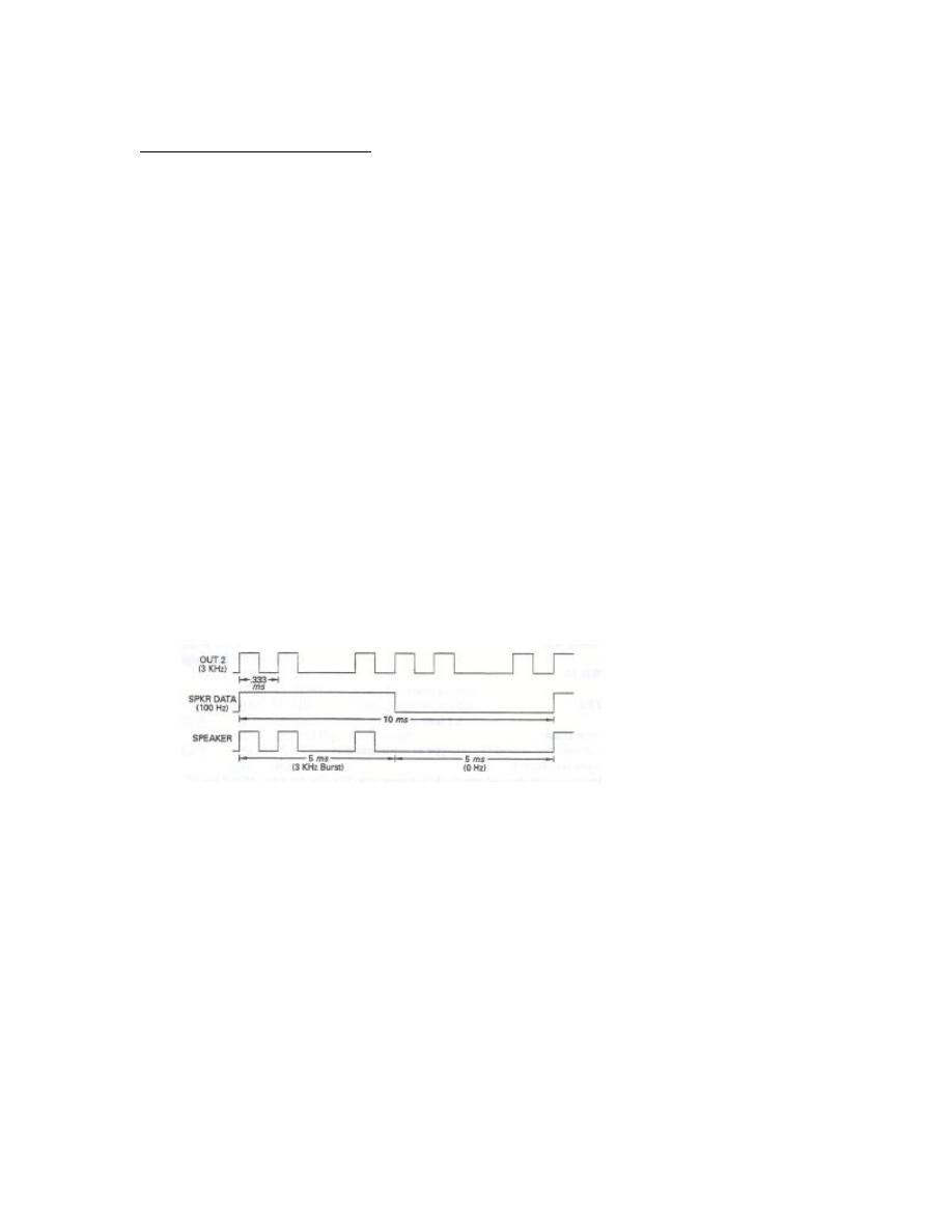
43.
DMA page register
Contents
1
0AH
2
0BH
3
0CH
Instruction sequence:
MOV AL,0AH
;Init. channel 1 page register
OUT 81H,AL
MOV AL,0BH
;Init. channel 2 page register
OUT 82H,AL
MOV AL,0CH
;Init. channel 3 page register
OUT 83H,AL
Section 12.7
44.
Timer interrupt frequency = 1/54.93 6 ms = 18.2 Hz
Refresh request frequency = 1/15.12
µ
s = 66.14 KHz
45.
Counter 1 divisor = 1.1 M/18.2 = 60,440
46.
When the speaker is to be used, the 8088 must write logic 1 to bit 0 of port B of the
8255A to produce the signal TIM 2 GATE SPK that enables the clock for timer 2. Pulses
are now produced at OUT
2
. When a tone is to be produced by the speaker, the 8088
outputs the signal SPKR DATA at pin 1 of port B. This signal enables the pulses output
at OUT
2
to the 75477 driver. The output of the driver is supplied to the speaker.
Changing the count in timer 2 can change the frequency of the tone.
47.
48.
MOV AL, SW1_EN
;Enable SW1 buffer
OUT 61H, AL
IN
AL, 60H
:Input SW1
MOV [SW1_LOC], AL
;Save SW1
MOV AL, SW1_DIS
;Disable SW1 buffer
OUT 61H, AL
; Where, SW1_EN is a byte with MSB = 1
;
SW_DIS is a byte with MSB = 0
;
SW1_LOC is a location where SW1 is saved.
Section 12.8
49.
KBD IRQ is an output that is used as an interrupt to the MPU and, when active, it
signals that a keyscan code needs to be read.

50.
KBR_SRV: PUSH AX
;Save register to be used
MOV AL, KEYBDCLK_LOW
;Hold keyboard clock low
OUT 61H, AL
MOV AL, SR_EN
;Enable the shift register output
OUT 61H, AL
IN
AL, 60H
;Input the key code
MOV [KBD_LOC], AL
;Save the keycode
MOV AL, KEYBDCLK_EN
;Release the keyboard clock
OUT 61H, AL
POP AX
;Restore register
IRET
;Return
; Where, KEYBDCLK_LOW is a byte with bit 6 = 0
;
KEYBDCLK_EN is a byte with bit 6 = 1
;
SR_EN is a byte with the MSB = 0
;
KBD_LOC is a byte location where the key code is saved
Section 12.9
51.
I/O channel slots provide the system interface to add -on cards. Five 62-pin card slots
are provided on the system board.
52.
A
10
. Active high.
Chapter 13
Section 13.1
1.
Prototype circuit.
2.
A circuit card that is used to prototype an experimental circuit.
3.
Solderless breadboard.
4.
An extender card is plugged into the I/O channel slot of the PC (ISA slot for a PC/AT)
and the card to be tested is plugged into the top of the extender card. This elevates the
circuits on the board above the housing of the PC to permit easy access for testing.
5.
Bus interface module, I/O expansion bus cables, breadboard unit
Section 13.2
6.
Switches, LEDs, and a speaker.
7.
The INT/EXT switch must be set to the EXT position.
8.
One.
9.
26 AWG.
10.
The horizontal row marked with a line.
11.
A
31
through A
12
.
12.
Test for continuity between two points in a circuit; the buzzer sounds if continuity
exists between the test points.

13.
Logic 0 lights the green LED; logic 1 lights the red LED; and the high -Z level lights
the amber LED.
14.
The red LED marked P blinks.
Section 13.3
15.
74LS688, 74LS138, and 74LS32.
16.
IOWX31E----
17.
A
10
through A
15
.
18.
Yes; IOWX31E----
19.
The select outputs of the 74LS138 are gated with either IOR ---- or IOW---- in
74LS32 OR gates. These signals are active only during an I/O cycle.
20.
D
7
D
6
D
5
D
4
D
3
D
2
D
1
D
0
= 00001111
2
21.
Yes
22.
MOV DX,31DH
;Read the switches
IN AL,DX
;Mask off all but S1 and S0
AND AL,3H
CMP AL,3H
JZ SERVE_3
;Branch to SERVE_3 of S1 & S1 are closed
23.
The setting of switch 7 is polled waiting for it to close.
24.
LED 0; LED 7.
25.
Lights LEDs 0 through 3.
26.
MOV DX,31EH
;Select LED port address
MOV AL,01H
;Select code for 1st LED
SCAN: OUT DX,AL
;Write to light next LED
MOV CX,0FFFFH ;Wait a while
DELAY: DEC CX
JNZ DELAY
ROL AL,1
;Select code for next LED
JMP SCAN
;Repeat
27.
The LEDs are lit in a binar y counting pattern.
28.
75477.
29.
Change MOV CX,0FFFFH to MOV CX,7FFFH.
Section 13.4
30.
IN AL,8000H reads the switch setting into the LSB of AL. Logic 0 in a bit position
indicates that the corresponding switch is open.
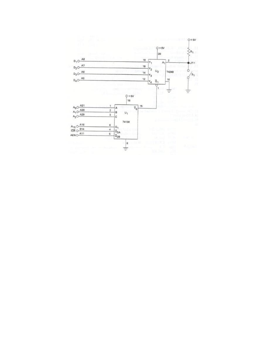
31.
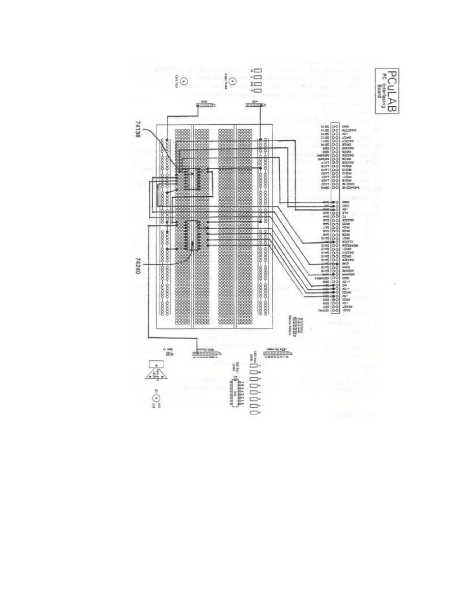
31.
(Continued)

32.
Diagnostic program.
33.
IC test clip.
34.
Logic probe, multimeter, and oscilloscope.
35.
Whether the test point is at the 0, 1, or high -Z logic state, or if it is pulsating.
36.
The multimeter reads the actual voltage present at a test point.
37.
Amount of voltage, duration of the signal, and the signal waveshape.
38.
The signal waveshape pattern repeats at a regular interval of time.
39.
Troubleshooting.
40.
Software debug.
41.
Hardware troubleshooting.
42.
i)
Programming of VLSI peripherals
ii)
Addresses of I/O devices or memory locations
iii)
Algorithm implementation
43.
i)
Check to verify that correct pin numbers are marked into the schematic diagram.
ii)
Verify that the circuit layout diagram correctly impleme nts the schematic.
iii)
Check that the ICs and jumpers are correctly installed to implement the circuit.
44.
Power supply voltages.
45.
Test point Switch open Switch closed
1 1 0
2 1 0
3 Pulse Pulse
46.
The jumper from the switch to the junction of the resistor and pin 1 of the 74LS240 is
not making contact.
Section 13.5
47.
Address bus, data bus, and control-bus signals.
48.
Digital logic analyzer.
49.
Oscilloscope
Logic analyzer______________
i)
Requires periodic signal
i)
Can display periodic or
to display
nonperiodic signals
ii)
Small number of channels
ii)
Large number of channels
iii)
Displays actual voltage
iii)
Displays logic values
values
iv)
Generally does not store
iv)
Stores signals for
the signals for display
display
v)
Simple trigger condition
v)
Trigger signal can be a
using a single signal
combination of a number of
signals

Chapter 14
Section 14.1
1.
HMOSIII.
2.
125,000.
3.
PLCC, LCC, and PGA.
Section 14.2
4.
Bus unit , instruction unit, execution unit, and address unit.
5.
24 bits, 16 bits.
6.
Demultiplexed address and data buses.
7.
6 bytes.
8.
Address generation, address translation, and address checking.
9.
The queue holds the fetched instructions for the execu tion unit to decode and perform
the operations that they specify.
Section 14.3
10.
5×.
11.
That an 8086 object code program can run on the 80286.
12.
Machine status word register (MSW).
Section 14.4
13.
Saves the contents of various registers of the processor such as AX, SP, and so forth,
on the stack.
14.
DI, SI, BP, SP, BX, DX, CX, and AX.
15.
Data area on the stack for a subroutine to provide space for the storage of local
variables, linkage to the calling subroutine, and the return address.
16.
32 bytes for data + 10 bytes for the previous and current frame pointers; 4.
17.
A word of data from the word size port at address 1000H is input to the memory
address 1075H:100H. The SI register is incremented to 102H, and CX is decremented by
2.
18.
The 16 bytes of data in the range 1075H:100H through 1075H:0F0H are output one
after the other to the byte-wide output port at I/O address 2000H. Each time a byte is
output, the count in the CX register and the pointer in SI are decremented by 1. The
output sequence is repeated until the count in CX is 0.
19.
The instruction tests if VALUE lies between 0000H and 00FFH. If it is outside these
bounds, interrupt 5 occurs.
Section 14.5
20.
20-bits, 1 Mbyte; 24-bits, 16 Mbyte; 1 GByte.
21.
I/O write (out put bus cycle).

22.
Byte transfer over the upper eight data bus lines.
23.
No, it is one bit of a status code that must be decoded to produce an interrupt
acknowledge signal.
24.
HOLD and HLDA.
25.
80287.
Section 14.6
26.
M/IO----, S
1
----, S
0
----.
27.
IOWC----
28.
DT/R----, ALE, and DEN.
29.
1.
Section 14.7
30.
8 MHz, 10 MHz, and 12.5 MHz; 80286, 80286-10, and 80286-12, respectively.
31.
25 MHz.
32.
CLK and PCLK; 10 MHz and 5 MHz.
Section 14.8
33.
Four clocks; 400 ns.
34.
Send-status state, 80286 outputs the bus status code to the 82C288 and in the case of
a write (or output) bus cycle it also outputs data on the data bus.
35.
Perform-command state; external devices accept write data from the bus, or in the
case of a read cycle, place data on the bus.
36.
In Fig. 14.26(a) address n becomes valid in the T
c
state of the prior bus cycle and then
the data transfer takes place in the next T
c
state. Also, at the same time that data transfer n
occurs address n + 1 is output on the address bus. This shows that due to pipelining the
80286 starts to address the next storage location that is to be accessed while it is still
reading or writing data for the previously addressed storage location.
37.
An idle state is a period of no bus activity that o ccurs because the prefetch queue is
already full and the instruction currently being executed requires no bus activity.
38.
An extension of the current bus cycle by a period equal to one T
s
state because the
READY---- input was tested and found to be logi c 1; 600 ns.
Section 14.9
39.
The bus controller produces the appropriately timed command and control signals
needed to control transfers over the data bus. The decoder decodes the higher -order
address bits to produce chip-enable signals. The address la tch is used to latch and buffer
the lower bits of the address and chip -enable signals. The data bus buffer/transceiver
controls the direction of data transfers between the MPU and memory subsystem.
40.
110; MWTC----.

41.
Odd-addressed byte, even-addressed byte, even-addressed word, and odd-addressed
word. One bus cycle is required for all types of cycles, except the odd -addressed word
cycle, which requires two bus cycles.
42.
500 ns; 1
µ
s.
43.
Odd-addressed byte.
44.
a.
At the beginning of
φ
2
of the T
c
state in the previous bus cycle, the address, M/IO ----
and COD/INTA---- signals for the byte-write bus cycle are output.
b.
Status code S----
1
S----
0
equal to 10 is output on the status bus at the beginning of
φ
1
of
the write cycle and is maintained thro ughout the T
s
state. On the falling edge of CLK in
the middle of T
s
the 82C288 bus controller samples the status lines and the write cycle
bus control sequence is started.
c.
At the beginning of
φ
2
of T
s
, ALE is switched to logic 1. This pulse is used to latch the
address. Also DEN is switched to 1 to enable the data bus transceivers and DT/R ---- is
left at the
transmit level to set the transceivers to output data to the memory subsystem.
d.
At the beginning of
φ
2
in the T
s
state the byte of data to be written to memory is output
on bus lines D
0
through D
7
.
e.
At the start of
φ
1
of the T
c
state, MWTC---- is switched to its active 0 logic level to
signal the memory subsystem to read the data off the bus.
f.
Late in T
c
the 80286 and 82C288 test the logic level of READY ----. If it is logic 0, the
write cycle is completed.
45.
320 ns.
46.
480 ns.
Section 14.10
47.
M/IO----.
48.
82C288.
49.
The decoder is used to decode several of the upper I/O address bits to produce the
I/OCE---- signals. The latch is used to latch the lower -order address bits and I/OCE----
outputs of the decoder. The bus controller decodes the I/O bus commands to produce the
I/O and bus control signals for the I/O interface. The bus transceivers control the
direction of data transfer over the bus.
50.
600 ns.
51.
1.2
µ
s.
52.
During the T
c
state of the previous bus cycle, the 80286 outputs the I/O address along
with BHE---- = 0 and M/IO---- = 0. The address decoder decodes some of the address
bits to produce I/O chip enable sig nals. At the beginning of the T
s
state of the output
cycle, S----
1
S----
0
= 10 is output to signal that an output operation is in progress. The
82C288 decodes this bus status code and starting at
φ
2
of the T
s
state a pulse is output at
ALE. This pulse is us ed to latch the I/O address and chip enable signals into the address
latch. At the same time DEN is switched to 1 and DT/R ---- is held at the transmit level
(logic 1). Therefore, the bus transceivers are enabled and set up to pass data from the
80286 to I/O port. Finally, at the beginning of the T
c
state the bus controller switches
IOWC---- to logic 0 to signal the I/O device to read data off the bus.

Section 14.11
53.
Hardware interrupts, software interrupts, internal interrupts and exceptions, software
interrupts, and reset.
54.
0 through 255.
55.
Interrupt vector table; interrupt descriptor table.
56.
2 words.
57.
Interrupt descriptor table register, 0.
58.
CS
3
= A000H and IP
3
= A000H.
59.
INTR is the interrupt request signal that must be applied to the 80286 MPU by the
external interrupt interface circuitry to request service for an interrupt -driven device.
When the MPU acknowledges this request, it outputs an interrupt acknowledge bus status
code on M/IO---- S----
1
S----
0
, and this code is decoded by the 82C288 bus controller to
produce the INTA---- signal. INTA---- is the signal that is used to tell the external device
that its request for service has been granted.
60.
8.
61.
Divide Error,
Single step,
Breakpoint,
Overflow error,
Bounds check,
Invalid opcode,
Processor extension not available,
Interrupt table limit to small,
Processor extension segment overrun,
Segment overrun,
Processor extension error.
62.
Vectors 0 through 16.
Chapter 15
Section 15.1
1.
80386DX and 80386SX.
2.
32 bit registers and a 32-bit data bus; 32 bit registers and a 16 -bit data bus.
3.
39; 49.
4.
Real-address mode, protected-address mode, and virtual 8086 mode.
Section 15.2
5.
Bus unit, prefetch unit, decode unit, execution unit, segment unit, and page unit.
6.
32 bit, 32 bit.
7.
Separate address and data buses.
8.
16 bytes.
9.
Prefetch unit.

10.
6 word
×
64 bit.
11.
Translation lookaside buffer.
Section 15.3
12.
5
×
13.
Object code compatible means that programs and operating systems written for the
8088/8086 will run directly on the 80386DX and 80386SX in real -address mode.
14.
32 bits; 16 bits.
15.
FS, GS, and CR
0
registers.
Section 15.4
16.
MOV EBX,CR1
17.
Double precision shift left.
18.
The byte of data in BL is sign -extended to 32 bits and copied into register EAX.
19.
MOVZX EAX, [DATA_WORD].
20.
The first 32 bits of the 48 -bit pointer starting at memory address
DATA_F_ADDRESS are loaded into EDI and the next 16 bits are loaded into the FS
register.
21.
(a) (AX) = F0F0H, (CF) = 1.
(b) (AX) = F0E0H, (CF) = 1.
(c) (AX) = F0E0H, (CF) = 1.
22.
Set byte if not carry; (CF) = 0.
Section 15.5
23.
Global descriptor table register, interrup t descriptor table register, task register, and
local descriptor table register.
24.
LIMIT and BASE.
25.
Defines the location and size of the global descriptor table.
26.
GTD
START
= 210000H, GDT
END
= 2101FFH; SIZE = 512 bytes; DESCRIPTORS =
64
27.
System segment descriptors.
28.
Interrupt descriptor table register and interrupt descriptor table.
29.
0FFFH
30.
Interrupt gates.
31.
Local descriptor table.
32.
Selector; the LDT descriptor pointed to by the selector is cached into the LDT cache.
33.
CR
0
.
34.
PE
35.
(MP) = 1, (EM) = 0, and (ET) = 1.
36.
Task switched.
37.
Switch the PG bit in CR
0
to 1.
38.
CR
3
.
39.
4Kbyte

40.
Page frame addresses.
41.
Selector; selects a task state segment descriptor.
42.
The selected task state segment descriptor is loaded into this register for on-chip
access.
43.
BASE and LIMIT of the TSS descriptor.
44.
Code segment selector register; data segment selector register.
45.
RPL = 2 bits
TI = 1 bit
INDEX = 13 bits
46.
Access the local descriptor table.
47.
00130020H
48.
NT = nested task; RF = resume flag.
49.
Level 2
50.
48 bits.
51.
Selector and offset.
52.
4Gbyte, 1 byte
53.
64Tbyte, 16,384 segments.
54.
32Tbyte, 8192.
55.
Task 3 has access to the global memory address space and the task 3 local address
space, but it cannot access either the task 1 local address space or task 2 local address
space.
56.
Memory management unit.
57.
The first instruction loads the AX register with the selector from the data storage
location pointed to by SI. The second instruction loads the selector into the code segment
selector register. This causes the descriptor pointed to by the selector in CS to be loaded
into the code segment descriptor cache.
58.
00200100H
59.
1,048,496 pages; 4096 bytes long.
60.
Offset field = 20 bit; page field = 10 bit; directory field = 10 bit.
61.
Cache page directory and page table pointers on-chip.
62.
4Kbytes; offset of the linear address.
Section 15.6
63.
8, BASE = 32-bits, LIMIT = 20-bits, ACCESS RIGHTS BYTE = 8-bits,
AVAILABLE = 1 bit, and GRANULARITY = 1 bit.
64.
CS, DS, ES, FS, GS, or SS; GDTR or LDTR.
65.
LIMIT = 00110H, BASE = 00200000H.
66.
ACCESS RIGHTS BYTE = 1AH
P = 0 = Not in physical memory
E = 1, R = 1 = Readable code segment
A = 0 = Descriptor is not cached.
67.
00200226H
68.
20 most significant bits of the base address of a page table or a page frame.
69.
R/W = 0 and U/S = 0 or R/W = 1 and U/S = 0.

70.
Page fault.
71.
Dirty bit.
Section 15.7
72.
(INIT_GDTR) = FFFFH
(INIT_GDTR + 2) = 0000H
(INIT_GDTR + 4) = 0030H
73.
LMSW AX
;Get MSW
AND AX,0FFF7H
;Clear task-switched bit
SMSW AX
;Write new MSW
74.
MOV BX, 2F0H
;(BX) = selector
LLDT BX
;Load local descriptor table register with selector
Section 15.8
75.
The running of multiple processes in a time -shared manner.
76.
A collection of program routines that perform a specific function.
77.
Local memory resources are isolated from global memory resources and tasks are
isolated from each other.
78.
The descriptor is not loaded; instead, an error condition is signaled.
79.
Level 0, level 3.
80.
Level 3.
81.
LDT and GDT.
82.
Use of a separate LDT for each task.
83.
Level 0.
84.
Current privilege level, requested privilege level.
85.
A task can access data in a data segment at the CPL and at all lower privilege levels,
but it cannot access data in segments that are at a higher privilege level.
86.
Level 3.
87.
A task can access code in segments at the CPL or at higher privilege levels, but
cannot modify the code at a higher privilege level.
88.
Level 0, level 1, and level 2.
89.
The call gate is used to transfer control within a task from code at the CPL to a
routine at a higher privilege level.
90.
Execution of this instruction initiates a call to a routine at a higher privilege level
through the call gate pointed to by address NEW_ROUTINE.
91.
Identifies a task state segment.
92.
Defines the state of the task that is to be initiated .
93.
The state of the prior task is saved in its own task state segment. The linkage to the
prior task is saved as the back link selector in the first word of the new task state
segment.
94.
TR
Section 15.9

96.
Bit 17.
97.
Active, level 3.
98.
Yes.
99.
Yes.
Section 15.10
100.
Floating-point math coprocessor and code and data cache memory.
101.
The 80486SX does not have an on-chip floating-point math coprocessor.
102.
136; 249.
103.
32 bytes.
104.
Complex instruction set computer; reduced instruction set computer, complex
reduced instruction set computer.
105.
Small instruction set, limited addressing modes, and single clock execution for
instructions.
106.
CRISC
107.
Cache disable (CD) and not write-through (NW).
108.
Little Endian.
109.
F0F0H.
110.
MOV CX, COUNT
MOV SI, BIG_E_TABLE
MOV DI, LIT_E_TABLE.
NXTDW:
MOV EAX, [SI]
SWAP EAX
MOV [DI], EAX
ADD SI, 04H
ADD DI, 04H
LOOP NXTDW
111.
XADD [SUM], EBX
(EAX) (SUM)
01H 00H
01H 01H 1st execution
01H 02H 2nd execution
02H 03H 3rd execution
03H 05H 4th execution
112.
Since the contents of the destination op erand, memory location DATA, and register
AL are the same, ZF is set to 1 and the value of the source operand, 22
16
is copied into
destination DATA.
113.
Alignment check (AC); bit 18.
114.
Cache disable (CD) and not write -through (NW).
115.
INVD
116.
WBINVD initiates a write back bus cycle instead of a flush bus cycle.
117.
Page cache disable (PCD) and page write transparent (PWT).
Section 15.11

118.
Integer
Fraction
9
÷
2 à 1
2
×
.5
4
÷
2 à 0
2
×
1.0 à 1
2
÷
2 à 0
.5 = .1
2
1
÷
2 à 1
9 = 1001
2
−
9.5 =
−
1001.1
2
=
−
1.0011
×
2
+3
119.
Single precision number = 32 bits, double precision number = 64 bits, and extended
precision number = 80 bits
120.
Sign, biased exponent, and fractional significand (extended has full significand).
121.
Sign = 1
Biased exponent = +3 + 127 = 00000011
2
+ 01111111
2
= 10000010
Fractional significand = 00110000000000000000000
−
1.0011
×
2
+3
=
1 10000010 00110000000000000000000;
−
1.0011
×
2
+3
=
C1180000H
122.
8, R0 through R7, ST(0) through ST(7).
123.
R
2
, 5, R
5
.
124.
TOP is decremented so that the new top of stack is R
4
and the value from the old
ST(2), R
7
, is copied into R
4
.
125.
(DATA4_64B)
−
(DATA3_64B)
à DATA5_64B
−
10.75
−
(
−
2.5)
=
−
10.75
+
2.5
=
−
8.25
= 8.25
8.25 = 1000.01
2
= 1.00001
×
2
+3
Sign = 0
Biased exponent = 00000000011
2
+ 01111111111
2
= 10000000010
Fractional significand = 0000100000000000000000000000000000000000000000000000
8.25 = 0 10000000010 0000100000000000000000000000000000000000000000000000
8.25 = 0100000000100000100000000000000000000000000000000000000000000000
2
8.25 = 4020800000000000H
Section 15.12
126.
64 bits.
127.
A microprocessor architecture that employs more than one execution unit.
128.
735.
129.
2; U pipe and V pipe.
130.
Separate code and data caches; write-through or write-back update methods; dual
port ALU interface.
131.
5 to 10 times faster.
132.
ID, VIP, and VIF.
133.
Page size extensions, 1M 32-bit entries.
134.
Machine check exception.
135.
Compare and exchange 8 bytes (CMPXCHG8B), CPU identification (CPUID), and
read from time stamp counter (RDTSC).
136.
ZF
←
0; (EDX:EAX)
←
(TABLE) = 11111111FFFFFFFF
16
137.
Machine check type (MCT).

Section 15.13
138.
Single instruction multiple data.
139.
Packed byte, packed word, packed double word, and packed quad-word; 8
×
8-bit,
4
×
16-bit, 2
×
32-bit, and 1
×
64-bit.
140.
64-bits wide; MM
0
through MM
7
.
141.
(a) Byte 7 = FFH, Byte 6 = 00H, Byte 5 = 12H, B yte 4 = 34H, Byte 3 = 56H, Byte 2 =
78H, Byte 1 = ABH, Byte 0 = CDH.
(b) Word 3 = FF00H, Word 2 = 1234H, Word 1 = 5678H, Word 0 = ABCDH
(c) Double word 1 = FF001234H Double word 0 = 5678ABCDH
142.
Byte 7 FFH + 00H = FFH
Byte 6 FFH + 01H = 100H à FFH due to saturation
Byte 5 FFH + 00H = FFH
Byte 4 FFH + 02H = 101H à FFH due to saturation
Byte 3 12H + 87H = 99H
Byte 2 34H + 65H = 99H
Byte 1 56H + 43H = 99H
Byte 0 78H + 21H = 99H
MM
3
= FFFFFFFF99999999H
143.
Data is compared as signed numbers. This gives
Double word 1 FFFFFFFFH > 00010002H = False à 00000000H
Double word 0 12345678H > 876554321H = True à FFFFFFFFH
MM
3
= 00000000FFFFFFFFH
144.
MM
5
Byte 7 01H
Byte 6 FFH à FFH Unsigne d saturation overflow
Byte 5 00H à 00H Unsigned saturation underflow
Byte 4 23H à FFH Unsigned saturation overflow
MM
6
Byte 3 00H à 00H Unsigned saturation underflow
Byte 2 00H à 00H Unsigned saturatio n underflow
Byte 1 00H
Byte 0 21H à FFH Unsigned saturation overflow
MM
6
= 01FF00FF000000FFH
Chapter 16
Section 16.1
1.
CHMOSIII.
2.
275,000.
3.
INTR.
Section 16.2

4.
20-bits, 1Mbyte; 32-bits, 4Gbyte; 64Tbyte.
5.
Byte, D
0
through D
7
, no.
6.
1011, 0111, 0011.
7.
I/O data read.
8.
HOLD and HLDA.
9.
80387DX numeric coprocessor.
Section 16.3
10.
16 MHz, 20 MHz, 25 MHz, and 33 MHz; 80386DX -16, 80386DX-20, 80386DX-25,
and 80386DX-33, respectively.
11.
F12.
12.
50 MHz.
Section 16.4
13.
40 ns.
14.
Pipelined and nonpipelined.
15.
In Fig. 16.11 address n becomes valid in the T
2
state of the prior bus cycle and then
the data transfer takes place in the next T
2
state. Also, at the same time that data transfer n
occurs, address n+1 is output on the address bus. This shows that during pipelining, the
80386DX starts to address the next storage location to be accessed while still reading or
writing data for the previously addressed storage location.
16.
An idle state is a period of no bus activity that occurs because the prefetch queue is
full and the instruction currently being executed does not require any bus activity.
17.
An extension of the current bus cycle by a period equal to one or more T states
because the READY--- input was tested and found to be logic 1.
18.
T
1
and T
2
.
19.
80 ns.
20.
160 ns.
Section 16.5
21.
Four independent banks each organized as 1G
×
8 bits; four banks each organized as
256K
×
8 bits.
22.
Types of data transfer No. of bus cycles
Byte transfer 1
Aligned word transfer 1
Misaligned word transfer 2
Aligned double-word transfer 1
Misaligned double-word transfer 2
23.
120 ns; 240 ns.
24.
Higher-addressed byte.
25.

The bus control logic produces the appropriately timed command and control signals
needed to control transfers over the data bus.
The address decoder decodes the higher -order address bits to produce chip-enable
signals.
The address bus latch is used to latch and buffer the lower bits of the address, byte -
enable signals, and chip -enable signals.
The bank write control logic determines to which memory banks MWTC --- is applied
during write bus cycles.
The data bus transceiver/buffer controls the direction of data transfers between the
MPU and memory subsystem and supplies buffering for the data bus lines.
26.
M/IO---D/C---W/R--- = 111
2
, all four, MWTC ---.
Section 16.6
27.
M/IO---
28.
Bus control logic.
29.
The I/O address decoder is used to decode several of the upper I/O address bits to
produce the I/OCE--- signals.
The I/O address bus latch is used to latch lower -order address bits, byte-enable
signals, and I/OCE--- outputs of the decoder.
The bus -control logic decodes I/O bus commands to produce the input/output and bus -
control signals for the I/O interface.
The data bus transceivers control the direction of data transfer over the bus, multiplex
data between the 32-bit microprocessor data bus and the 8-bit I/O data bus, and supplies
buffering for the data bus lines.
The I/O bank -select decoder controls the enabling and multiplexing of the data bus
transceivers.
30.
160 ns.
31.
320 ns.
32.
I/O map base; word offset 66H from the beginning of the TSS.
33.
BASE+8H; LSB (bit 0)
34.
1.
Section 16.7
35.
Interrupt vector table; interrupt descriptor table.
36.
Two words; four words.
37.
Interrupt descriptor table register; 0000000003FF
16
.
38.
B0H through B3H
39.
(a) Active; (b) privilege level 2; (c) interrupt gate; (d) B000H:1000H.
40.
010000
16
; 512 bytes; 64.
41.
In the protected mode, the 80386DX's protection mechanism comes into play and
checks are made to confirm that the gate is present; the offset is within the limit of the

interrupt descriptor table; access byte of the descriptor for the type number is for a trap,
interrupt, or task gate; and to assure that a privilege level violation will not occur.
42.
Divide error, debug, breakpoint, overflow error, bounds check, invalid opcode,
coprocessor not available, interrupt table limit to small, coprocessor segment overrun,
stack fault, segment overrun, and coprocessor error.
43.
Faults, traps, and aborts.
44.
Vectors 0 through 31.
45.
Fault
46.
Any attempt to access an operand that is on the stack at an address that is outside the
current address range of the stack segment.
47.
Double fault, invalid task state segment, segment not present, general protect ion
fault, and page fault.
Section 16.8
48.
INTR
49.
DP
0
, DP
1
, DP
2
, DP
3
, and PCHK----; even parity.
50.
BRDY---- = 0.
51.
Cache enable.
52.
BOFF----
53.
Four double words = 16 bytes; BRDY ---- = 0; 5 clock cycles.
54.
This means that the code o r data that is read from memory is copied into the internal
cache; KEN---- = 0; 4 double words = 16 bytes.
55.
Near to zero-wait-state operation even though the system employs a main memory
subsystem that operates with one or more wait states.
56.
First level.
57.
A bus cycle that reads code or data from the cache memory is called a cache hit.
58.
93.2%
59.
0.203 wait states/bus cycle.
60.
Four-way set associative.
61.
8Kbytes; line of data = 128 bits (16 bytes).
62.
Write-through.
63.
The contents of the internal cache are cleared. That is, the tag for each of the lines of
information in the cache is marked as invalid.
64.
Alignment check; gate 17.
Section 16.9
65.
Clock doubling and write-back cache.
66.
Snooping.
67.
Modify/exclusive/shared/invalid (MESI) protocol.
68.
HITM---- and 0.
69.
The WBWT---- input must be held at logic 1 for at least two clock periods before
and after a hardware reset.
70.
Clock tripling and 16Kbyte on-chip cache memory.
71.
435/68 = 6.4.

72.
3.3V dc.
Section 16.10
73.
3 million transistors.
74.
3.3V dc.
75.
D
45
is at pin A21; A
3
is at pin T17.
76.
8, 8, 1.
77.
Data parity and address parity; APCHK ---- = 0 address parity error and PCHK ---- =
0 data parity error.
78.
The current bus cycle has not run correct ly to completion.
79.
I/O write.
80.
It is a pipelined bus cycle.
81.
Two-way set associative.
82.
8Kbyte code cache; 8Kbyte data cache.
83.
256 bits (32 bytes).
84.
The write-through update method is used to write the data to external memory.
85.
Read hits access the cache, read misses may cause replacement, write hits update the
cache, writes to shared lines and write misses appear externally, write hits can change
shared lines to exclusive under control of WB/WT----, and invalidation is allowed.
Section 16.11
86.
Pentium
R
Pro processor
87.
5.5 million; 4.5 million.
88.
256Kbyte, and 512Kbyte.
89.
Both the code and data caches are 16Kbytes in size; they are organized four -way set-
associative.
90.
182
Section 16.12
91.
Celeron
TM
processor.
92.
386,213.
93.
533Mbytes/sec.
94.
1400Mbytes/sec.
95.
Single edge contact cartridge.
96.
4000 Mbytes/second
Section 16.13
97.
P6 microarchitecture; NetBurst
TM
microarchitecture.
98.
Forty two million transistors.
99.
133 MHz; 400 MHz.
100.
Execution trace cache.