Experiment (3): Bipolar Junction Transistor Characteristics Circuit
1
2016/2017
Study Objective:
(1) Understanding the structures and symbols of the transistors.
(2) Understand the characteristics of the transistors.
(3) Learning to judge the quality of transistor by using instruments.
Introduction:
1. New Terminology:
(a) β (h
fe
): The current gain when the transistor is connected as a CE.
β= I
C
/I
B
. The β value can be looked up from the data sheet, or
can be by experiment.
(b) α: The current gain when the transistor is connected as a CB circuit.
α= I
C
/I
E
= β /(1+ β).
(c) Transistor: The current that flows through C and E terminals of the
transistor will be changed in response to I
B
. In other words, I
B
will control the internal resistor of CE. The transistor is
substantially a "transferable resistor" that can transfer the
input signal into the magnitude of resistor. Transistor is
therefore a combined word of "transfer" and "resistor".
2. Basic Principle:
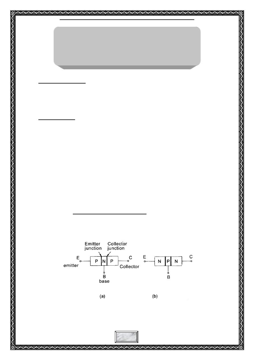
A) Structures and characteristics of the transistors
i) Structures of the transistors
The transistors can be classified into two major types -
PNP and NPN type. Their structure diagrams are respectively
shown in Fig. 1 (a) (b). E (Emitter), B (Base) and C (Collector)
respectively represents the three terminals of the transistor.
Fig.1 Structure Diagram of Transistor
Experiment No. (3)
Bipolar Junction Transistor
Characteristics Circuit
Experiment (3): Bipolar Junction Transistor Characteristics Circuit
2
2016/2017
ii) Characteristics of the transistors
As shown in Fig. 2 (a), if a forward bias (P and N are
respectively connected to positive and negative polarity) is
applied across the terminals of E-B so that V
BE
will reach the
potential barrier (0.7V for silicon, and 0.2V for germanium), a
forward current I
B
will be generated between E-B. This forward
bias causes a substantial flow of current across the input
junction.
Since the base is very thin and is lightly doped a very
few of the holes recombine with the electrons in the base, and
the majority swept the reverse biased junction between base
and collector under the influence of the applied voltage on the
collector
As shown in Fig. 2 (b), we can see that:
(1) I
E
= I
B
+ I
C
, I
C
= βI
B
Fig. 2 (b),
(2) I
C
= αI
E
Fig. 2 (a),
Fig. 2 Bias Method for PNP Transistor
B) Symbols and Basic Circuits of the transistors
i) Symbol
Fig. 3 Symbols of the Transistor
Figure 3 shows the symbols of the transistor that have the following meaning:
(1) The arrow in the emitter used to differentiate between NPN and PNP.
The outward pointed arrow represents NPN type, and the inward
pointed arrow represented PNP type.
(2) Arrow is used to indicate the direction of the current.
Experiment (3): Bipolar Junction Transistor Characteristics Circuit
3
2016/2017
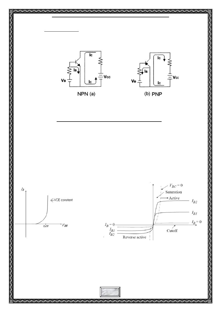
ii) Basic circuits
The basic bias and current direction of the NPN and PNP types are
respectively shown in Fig. 4 (a) and (b).
Fig. 4 Basic circuits for NPN & PNP
(iii) V-I characteristic curve of the transistor in CE
The transistor has two V-I characteristic curves:
1) Input Characteristic: If the collector-emitter voltage(V
CE
) is
kept constant, the curve of base current, I
B
, versus V
BE
is called the
input characteristic of transistor (Fig.5 (a)). This curve is similar
to the characteristic curve of a diode.
2) Output Characteristic: The other set of characteristic curves
are the output characteristic curves (Fig.5 (b)). These curves are
more important since they define the regions of operation of the
transistor (table(1) depicts these regions). These curves show the
relation between I
C
and V
CE
at each value of I
B
. As you can see, I
B
controls the collector current.
(a): Input Characteristics Curve (b): Output Characteristics Curve
Fig.5
V
CE
I
C
Experiment (3): Bipolar Junction Transistor Characteristics Circuit
4
2016/2017
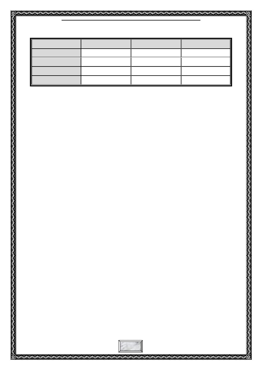
Table (1): operation regions of the transistor
Operating Region
BC Junction
BE Junction
Features
Cut-off
Reverse
Reverse
I
B
≈ I
C
≈ I
E
≈ 0
Saturation
Forward
Forward
V
CE
≈ 0
Active
Reverse
Forward
Amplifier
Reverse-active
Forward
Reverse
Limited Use
Experiment (3): Bipolar Junction Transistor Characteristics Circuit
5
2016/2017
Experiment Equipments:
(1) KL-200 Linear Circuit Lab.
(2) Experiment Module: KL-23002.
(3) Experiment Instrument: 1. digital multimeter.
2. Oscilloscope.
3. Signal generator.
(4) Tools: Basic hand tools.
(5) Materials: As indicated in the KL-23002.
Experiment items:
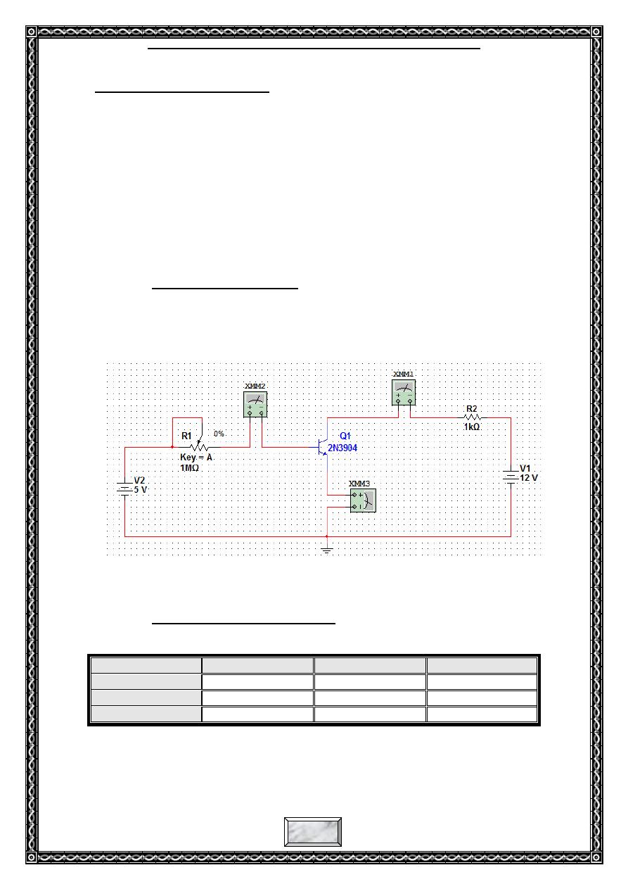
Item One :Experiment for Input Characteristics of NPN
Transistor and Measurements of l
E
, l
B
and l
C
.
Experiment Procedures:
(1) Connect the circuit shown in Fig. 7.
(2) Connect the ammeters to measure I
B
, I
C
and I
E
.
(3) Adjust VR1 (1MΩ) so that I
B
as table 2.
(4) View I
B
, I
C
and I
E
, and then record the result.
Fig. 7( NPN transistor )
Experiment Results for item 1:
Table(2)
I
B
I
C
(mA)
I
E
(mA)
β = I
C
/ I
B
20 µA
30 µA
50 µA
Experiment (3): Bipolar Junction Transistor Characteristics Circuit
6
2016/2017
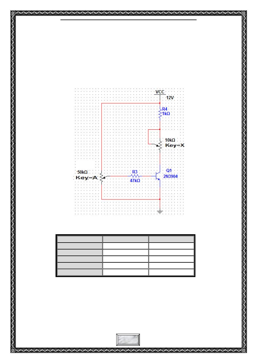
Item two : Experiment for input characteristics (relationship
between I
B
and V
BE
)
(1) Connect the circuit shown in Fig. 8 .
(2) Adjust VR2 (10kΩ) so that V
CE
= 10 V.
(3) Adjust VR3(50kΩ) so that I
B
will sequentially be( 2µA - 4µ A-
6µA- 8µA - 10µA. see table 3 .
(4) Referring to input characteristic curve, utilize the data shown in
Table 4 to plot the input characteristic curve .
Table (3)
V
CE
(V)
I
B
(µA)
V
BE
10
10
10
10
10
VR2
VR3
Experiment (3): Bipolar Junction Transistor Characteristics Circuit
7
2016/2017
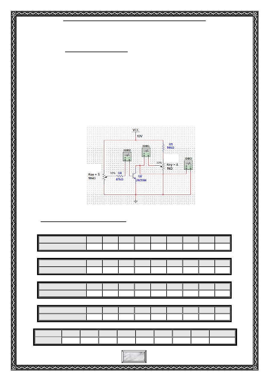
Item Three (3) Measurement and Plotting the Output
Characteristics Curve of BJT .
Experiment Procedures:
(1) Connect the circuit shown in Fig. 9 .
(2) Adjust VR2 (10kΩ) so that I
B
= 0 μA.
(3) Adjust VR1 (1kΩ) so that V
CE
will sequentially be ( 0.1V - 0.3V -
0.5V - 0.7V - 1.0V - 2.0V - 3.0V - 4.0V - 5.0V) and will
eventually approach to V
CC
. Record each corresponding I
C
value
in Table 5
(4) Adjust VR2 so that I
B
will be the values as indicated in Table 4,
then repeat Step (3) to measure V
CE
and I
C
. Record the result in
Table 4.
(5) Referring to output characteristic curve, utilize the data shown in
Table 4 to plot the output characteristic curve .
Fig. 9
Experiment Result for item three:
Table (4)
(a) I
B
= 0μA
V
CE
(V)
0.1V 0.2V
0.3
0.4V 0.5V 0.7V 1.0V 3.0V 5.0V
I
C
( mA)
(b) I
B
= 10μA(9.3)
V
CE
(V)
0.1V 0.2V 0.3V 0.4V 0.5V 0.7V 1.0V 3.0V 5.0V
I
C
( mA)
(c) I
B
= 20μA(21.4)
V
CE
(V)
0.1V 0.2V 0.3V 0.4V 0.5V 0.7V 1.0V 3.0V 5.0V
I
C
( mA)
(d) I
B
= 4
0μA
V
CE
(V)
0.1V 0.2V 0.3V 0.4V 0.5V 0.7V 1.0V 3.0V 5.0V
I
C
( mA)
(f) I
B
= 60μA
V
CE
(V)
0.1V
0.2V
0.3V
0.4V
0.5V
0.7V
1.0V
3.0V
5.0V
I
C
( mA)
VR2
VR1

Experiment (3): Bipolar Junction Transistor Characteristics Circuit
8
2016/2017
Discussion:
1. For Characteristics of the transistor, why is I
B
far smaller than I
C
?
2. Plot the V-I (input and output) characteristics curve for C.E of the
transistor for each cases NPN and PNP.
3. What are the regions indicated in the output characteristics of the
transistor? And For amplifier circuit, in which region should the transistor
operate?
4. what are the regions that transistor operate as switch? Answer with draws.
5. Choose the correct answer:
(a) P
C
means:
1. The power consumption in collector.
2. The power consumption in emitter.
3. The collector current.
(b) Select one of the following items that its maximum rated values can be
looked up from the specification manual.
1. I
E
.
2. I
B
.
3. P
C
.
(c) For BJT transistor, which is wrong among the following descriptions?
1. Transistor is a bipolar device.
2. Transistor is a voltage-control device.
3. Transistor is a current-control device.
(d) I
C
of the transistor is.
1. I
C
= β I
B.
2. I
C
= (1+β) I
B.
3. I
C
= I
E
+ I
B.
(e) Which one of the following items is represented by β?
1. Current gain factor.
2. Voltage gain factor.
3. Power gain factor.
(f) β value is equal to:
1. I
C
/I
E
.
2. I
C
/I
B
.
3. I
E
/I
B
.
6 . Write a conclusion for this experiment.