
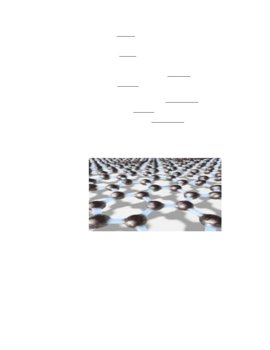
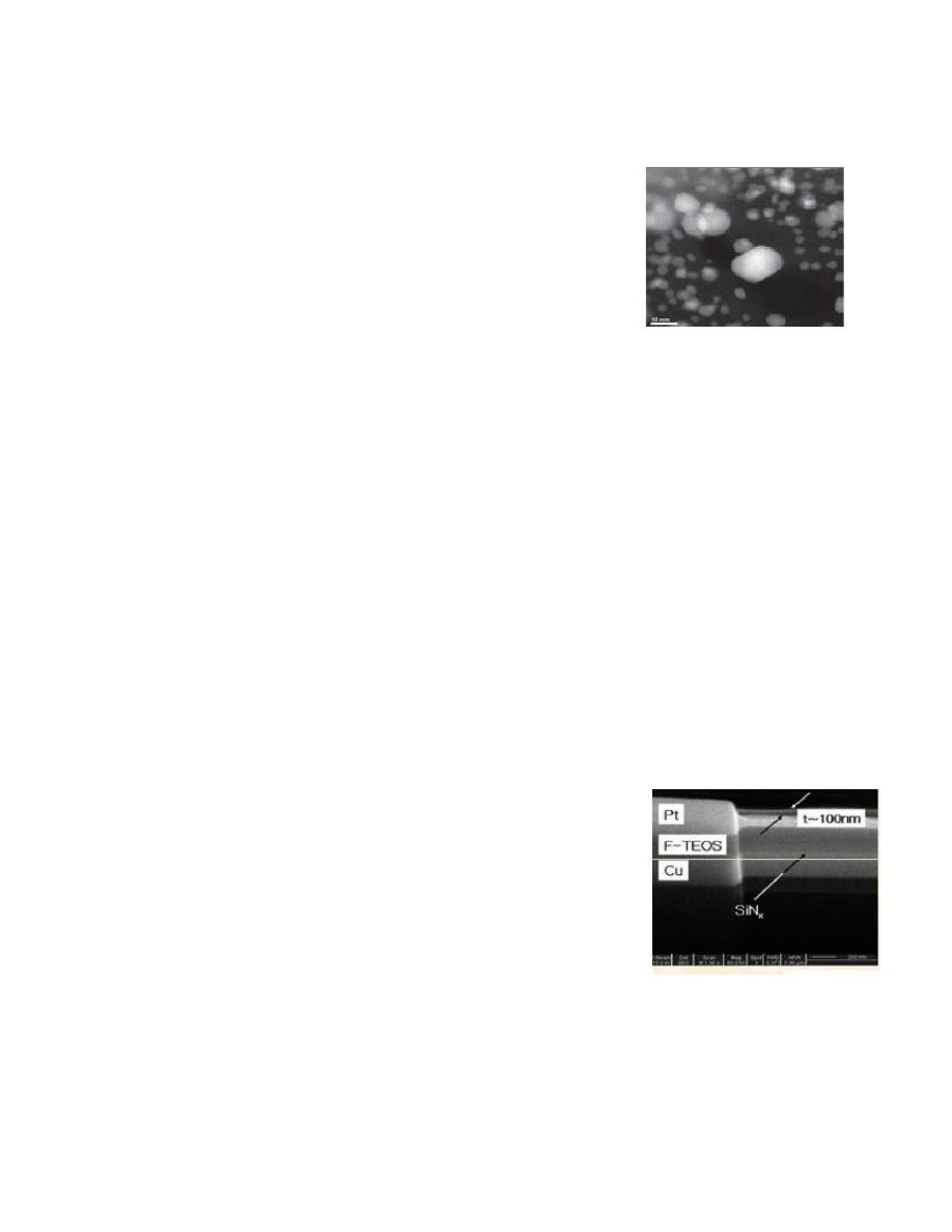
Nanomaterials
Contents
1- Introduction. ----------------------------------------- 4 hr.
1-1 Nanotechnology.
1-2 Environmental implications of nanotechnology.
1-3 Nano engineering .
2- Foundamentals of nanomaterials . ---------------- 6hr.
2-1 One-dimensional nanomaterials.
2-2 Two-dimensional nanomaterials .
2-3 Three-dimensional nanomaterials .
2-4 Matrix-reinforced and layered nanocomposites .
3- Properties at the nanomaterials . --------------------6hr.
3-1 Mechanical properties .
3-2 Optical Properties .
3-3 Electrical properties .
3-4 Magnetic properties .
5- Manufacturing of nanomaterials . --------------------4hr.
4-1 Form in place .
4-2 Mechanical.
4-3 Gas phase synthesis .
4-4 Wet chemistry.
`
5 - Application of nanomaterials . --------------------6hr.
5-1Fuel cells.
5-1-1 Carbon nanotubes - Microbial fuel cell .
5-2 Catalysis.
5-3 Phosphors for High-Definition TV.
5-4 Next-Generation Computer Chips.
5-5 Elimination of Pollutants.
5-6 Sun-screen lotion.
5-7 Sensors.

Lecture 1
(nano)
Nanotechnology
make use of very small objects or artefacts.
Nanomaterials are an increasingly important product of nanotechnologies.
They contain nanoparticles, smaller than 100 nanometres in at least one
dimension. Nanotechnology is the general term for designing and making
anything whose use depends on specific structure at the nanoscale –
generally taken as being 100 nanometres (100 millionths of a millimetre
or 100 billionths of a metre) or less. It includes devices or systems made
by manipulating individual atoms or molecules, as well as materials
which contain very small structures.
Nanotechnologies involve designing and producing objects or structures
at a very small scale, on the level of 100 nanometres (100 millionth of a
millimetre) or less.
Nanomaterials
are coming into use in healthcare, electronics,
cosmetics and other areas. Their physical and chemical properties often
differ from those of bulk materials, so they call for specialised risk
assessment. This needs to cover health risks to workers and consumers,
and potential risks to the environment.
Nanomaterials
are one of the main products of nanotechnologies – as
nano-scale particles, tubes, rods, or fibres
Nanomaterials
are usually considered to be materials with at least one
external dimension that measures 100 nanometres or less or with internal
structures measuring 100 nm or less. They may be in the form of
particles, tubes, rods or fibres. The nanomaterials that have the same

composition as known materials in bulk form may have different physico-
chemical properties than the same materials in bulk form, and may
behave differently if they enter the body. They may thus pose different
potential hazards.
This is currently done on a case by case basis, but risk assessment
methods need to be kept up to date as the use of nanomaterials expands,
especially as they find their way into consumer products
.
Aggregated nanomaterials also need to be assessed in this light as they
may exhibit properties that are similar to those of the single nanoparticles,
especially when they have an unusually large surface area for a given
amount of material.
Nanoparticles
are normally defined as being smaller that 100
nanometres in at least one dimension.
The number of products produced by nanotechnology or containing
nanomaterials entering the market is increasing. Current applications
include healthcare (in targeted drug delivery, regenerative medicine, and
diagnostics), electronics, cosmetics, textiles, information technology and
environmental protection. For example, nanosilver is appearing in a range
of products, including washing machines, socks, food packaging, wound
dressings and food supplements. Food supplements need especially close
scrutiny.
Characteristics of nanomaterials .
Descriptions of nanomaterials ought to include the average particle
size, allowing for clumping and the size of the individual particles and a

description of the particle number size distribution (range from the
smallest to the largest particle present in the preparation).
Detailed assessments may include the following:
1. Physical properties:
•
Their size, shape, specific surface area, and ratio of width and
height
•
Whether they stick together
•
Size distribution
•
How smooth or bumpy their surface is
•
Structure, including crystal structure and any crystal defects
•
How well they dissolve
2. Chemical properties:
•
Molecular structure
•
Composition, including purity, and known impurities or additives
•
Whether it is held in a solid, liquid or gas
•
Surface chemistry
•
Attraction to water molecules or oils and fats
These parameters should be assessed both for the nanomaterials as they
are made, and for nanomaterials as they are used (e.g. in the formulation
in any subsequent product). Measurements need to take account of the
way properties may change when nanomaterials are mixed with or
suspended in other substances.
It is particularly important to measure how quickly nanomaterials
dissolve in any liquid they are likely to come in contact with. Their small

size means they dissolve faster than the comparable bulk (large)
particulate material.
How can exposure to nanomaterials be measured?
The measurement methods to use depend on the kind of exposure.
The most reliable methods are for particles in the air. Nanoparticles may
also be in contact with solids and liquids, especially in consumer
products.
Current techniques to assess nanoparticle exposure are suitable for
personal or area-based monitoring, continuous or discontinuous use, and
basic characterisation of samples. However, data on airborne exposures
are scarce, and there have been few if any studies outside the workplace.
exposure estimates from food and consumer products also remain
difficult. Information on the presence of manufactured nanomaterials
comes from manufacturers. There is also limited information about
product use.
Effects of nanomaterials on the health
There is experimental evidence of a range of possible interactions
with biological systems and health effects of manufactured nanoparticles.
In experimental systems in the laboratory they can affect the formation of

the fibrous protein tangles which are similar to those seen in some
diseases, including brain diseases. Airborne particles might cause effects
in the lungs but also on the heart and blood circulation similar to those
already known for particulate air pollution. There is some evidence that
nanoparticles might lead to genetic damage, either directly or by causing
inflammation.
All these effects would depend on nanoparticles’ fate in the body.
Only a minimal amount of nanoparticle doses escape the lungs or
intestine, but long-term exposure could still mean a large number are
distributed round the body. Most are held in the liver or the spleen, but
some appear to reach all tissues and organs. There may also be entry into
the brain via the membranes inside the nose.
Nanotubes or rods with similar characteristics to asbestos fibres pose a
risk of the mesothelioma (a form of cancer of the pleura).
Environment effects of nanomaterials.
Wider use of nanomaterials will lead to increases in environmental
exposure. Little is known about how they may then behave in air, water
or soil. They may be concentrated in particular “hot spots”, either by
clumping together with minerals or by interaction with organic matter.
Like other pollutants, they may pass from organism to organism, and
perhaps move up food chains. As a result of their diversity, nanomaterials
may have a wide range of effects. Some kill bacteria or viruses.

Experiments so far have also shown possible harmful effects on
invertebrates and fish, including effects on behaviour, reproduction and
development. There is less research to date on soil systems and terrestrial
species, and it is not clear whether laboratory results relate to what may
happen out in the real world.
Assessment the risks from nanomaterials.
Existing risk assessment methods are generally applicable to
nanomaterials but specific aspects related to nanomaterials need more
development. They include methods for both estimating exposure and
identifying hazards. The highest potential risks come from free, insoluble
nanoparticles either dispersed in a liquid or as dust.
Risk assessment requires a detailed examination of properties, including:
•
Particle size
•
Surface area
•
Stability
•
Surface properties
•
Solubility
•
Chemical reactivity
Comparisons with well-known existing hazards may help inform risk
assessment. They include those from airborne fine particles, and asbestos
fibres.
The recommended approach to assess the risks from nanomaterials is still
the four stage risk assessment proposed by the SCENIHR in 2007. Today,
additional details can be added to this approach in the light of recent work
on evaluating possible harmful effects of nanomaterials, especially using
controlled laboratory tests (in vitro assays). These tests are useful for
screening and for investigating mechanisms of adverse effects. However,
tests using living organisms (in vivo assays) are also needed to improve
knowledge of possible risks to people and the environment.
Improvements are sought in the determination of exposures, and there is
an urgent need for long-term exposure studies.
Full evaluation of the potential hazards of most nanomaterials is still to
come. It will include estimation of exposure in normal use, abuse, waste
and recycling of products containing nanomaterials, and detailed
measurement of physical and chemical properties.
Lecture 2
(nano
)
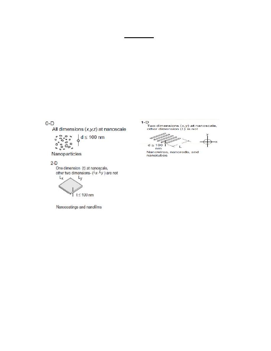
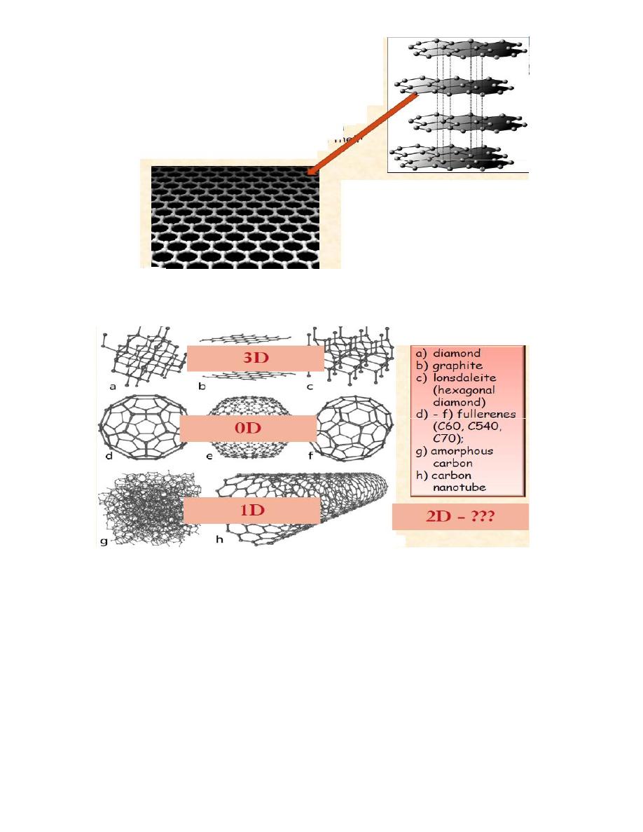
Classification.
* Classification is based on the number of dimensions, which are
not confined to the nanoscale range (<100 nm).
* (1) zero-dimensional (0-D),
* (2) one-dimensional (1-D),
* (3) two-dimensional (2-D), and
* (4) three-dimensional (3-D).
Zero-dimensional nanomaterials
* Materials wherein all the dimensions are measured within the
nanoscale (no dimensions, or 0-D, are larger than 100 nm).
* The most common representation of zero-dimensional
nanomaterials are nanoparticles.
*Nanoparticles can:
* Be amorphous or crystalline
* Be single crystalline or polycrystalline
* Be composed of single or multi-chemical elements
* Exhibit various shapes and forms
* Exist individually or incorporated in a matrix
* Be metallic, ceramic, or polymeric
Fundamentals of nanmaterials.
1
- One-dimensional nanomaterials
One dimension that is outside the nanoscale.
This leads to needle like-shaped nanomaterials.
1-D materials include nanotubes, nanorods, and
nanowires.
1-D nanomaterials
can be
Amorphous or crystalline
Single crystalline or polycrystalline
Chemically pure or impure
Standalone materials or embedded in within another medium
Metallic, ceramic, or polymeric
2-Two-dimensional nanomaterials
Two of the dimensions are not confined to the nanoscale.
2-D nanomaterials exhibit plate-like shapes.
Two-dimensional nanomaterials include nanofilms,
nanolayers, and nanocoatings.
2-D nanomaterials can be:
Amorphous or crystalline
Made up of various chemical compositions
Used as a single layer or as multilayer structures
Deposited on a substrate
Integrated in a surrounding matrix material
Metallic, ceramic, or polymeric
3-
Three-dimensional nanomaterials
Bulk nanomaterials are materials that are not confined to the
nanoscale in any dimension. These materials are thus characterized
by having three arbitrarily dimensions above 100 nm.
Materials possess a nanocrystalline structure or involve the
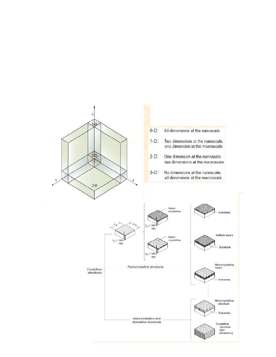
presence of features at the nanoscale.
In terms of nanocrystalline structure, bulk nanomaterials can be
composed of a multiple arrangement of nanosize crystals,
most typically in different orientations.
With respect to the presence of features at the nanoscale, 3-D
nanomaterials can contain dispersions of nanoparticles, bundles
of nanowires, and nanotubes as well as multinanolayers.
Three-dimensional space showing the relationships
among 0-D, 1-D, 2-D, and 3-D nanomaterials.
Summary
of 2-D and
3-D
crystalline
structures
4- Matrix-reinforced and layered Nanocomposites
These materials are formed of two or more materials with very
distinctive properties that act synergistically to create properties
that cannot be achieved by each single material alone. The matrix of
the nanocomposite, which can be polymeric, metallic, or ceramic, has
dimensions larger than the nanoscale, whereas the reinforcing phase is
commonly at the nanoscale.
5- Carbon
*Carbon is a basic element of life
*Carbon is special because of its ability to bond to many elements in
many different ways
* It is the sixth most abundant element in the
universe
|* The most known types of carbon materials:
diamond; graphite; fullerenes; and carbon
nanotubes
Carbon materials
Diamond and graphite are two graphite are two allotropes of
carbon: pure forms of the same element that differ in structure.
2s and 2p electrons available for bonding
6-DIAMOND
- chemical bonding is purely covalent
- highly symmetrical unit cell
- extremely hard
- low electrical conductivity
- high thermal conductivity (superior)
- optically transparent
- used as gemstones and industrial
grinding, machining and cutting
7-GRAPHITE
•
Layered structure with strong bonding within the planar layers
and weak, van der Waals bonding between layers
• Easy interplanar cleavage,
applications as a lubricant and for writing (pencils)
• Good electrical conductor
• Chemically stable even at high
temperatures
• excellent thermal shock
Applications:
Commonly used as heating elements (in non- oxidizing atmospheres),
metallurgical crucibles, casting molds, electrical contacts, brushes and
resistors, high temperature refractories, welding electrodes, air
purification systems, etc.
-Graphite
Graphite is a layered compound. In each layer,the carbon atoms are
arranged in a hexagonal lattice with separation of 0.142 nm, and the
distance between planes is 0.335 nm.The acoustic and thermal properties
of graphite arehighly anisotropic, since phonons propagate very
quickly along the tightly-bound planes, but are
slower to travel from one plane to another.
8-Graphene
Graphene is an one-atom-thick planar sheet of sp2-bonded carbon
atoms that are densely packed in a honeycomb crystal lattice. It can be
viewed as an atomic-scale chicken wire made of carbon atoms and their
bonds.
The carbon-carbon bond length in graphene is about 0.142 nm.
Graphene is the basic structural element of some carbon allotropes
including graphite, carbon nanotubes and fullerenes.
Allotropes of carbon
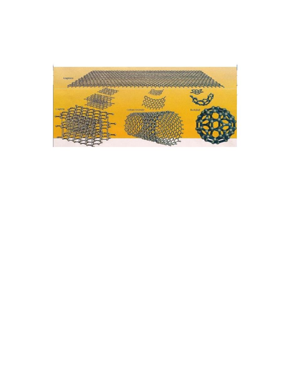
Graphene
The mother of all Graphites
SCIENCE, June 2010
* If there's a rock star in the world of materials, it's graphene: single-
atom–thick sheets of carbon prized for its off-the-charts ability to conduct
electrons and for being all but transparent.
* Those qualities make graphene a tantalizing alternative for use as a
transparent conductor, the sort now found in everything from computer
displays and flat panel TVs to ATM touch screens and solar cells.
* But the material has been tough to manufacture in anything larger than
flakes a few centimeters across.
* Now researchers have managed to create rectangular sheets of graphene
76 centimeters in the diagonal
direction and even use them to create a working touchscreen display
9-Quantum effects
*The overall behavior of bulk crystalline materials changes when the
dimensions are reduced to the nanoscale.
* For 0-D nanomaterials, where all the dimensions are at the nanoscale,
an electron is confined in 3-D space. No electrondelocalization (freedom
to move) occurs.
For 1-D nanomaterials, electron confinement occurs in 2-D,19 whereas
delocalization takes place along the long axis of the
nanowire/rod/tube.
* In the case of 2-D nanomaterials, the conduction electrons will
be confined across the thickness but delocalized in the plane of
the sheet.
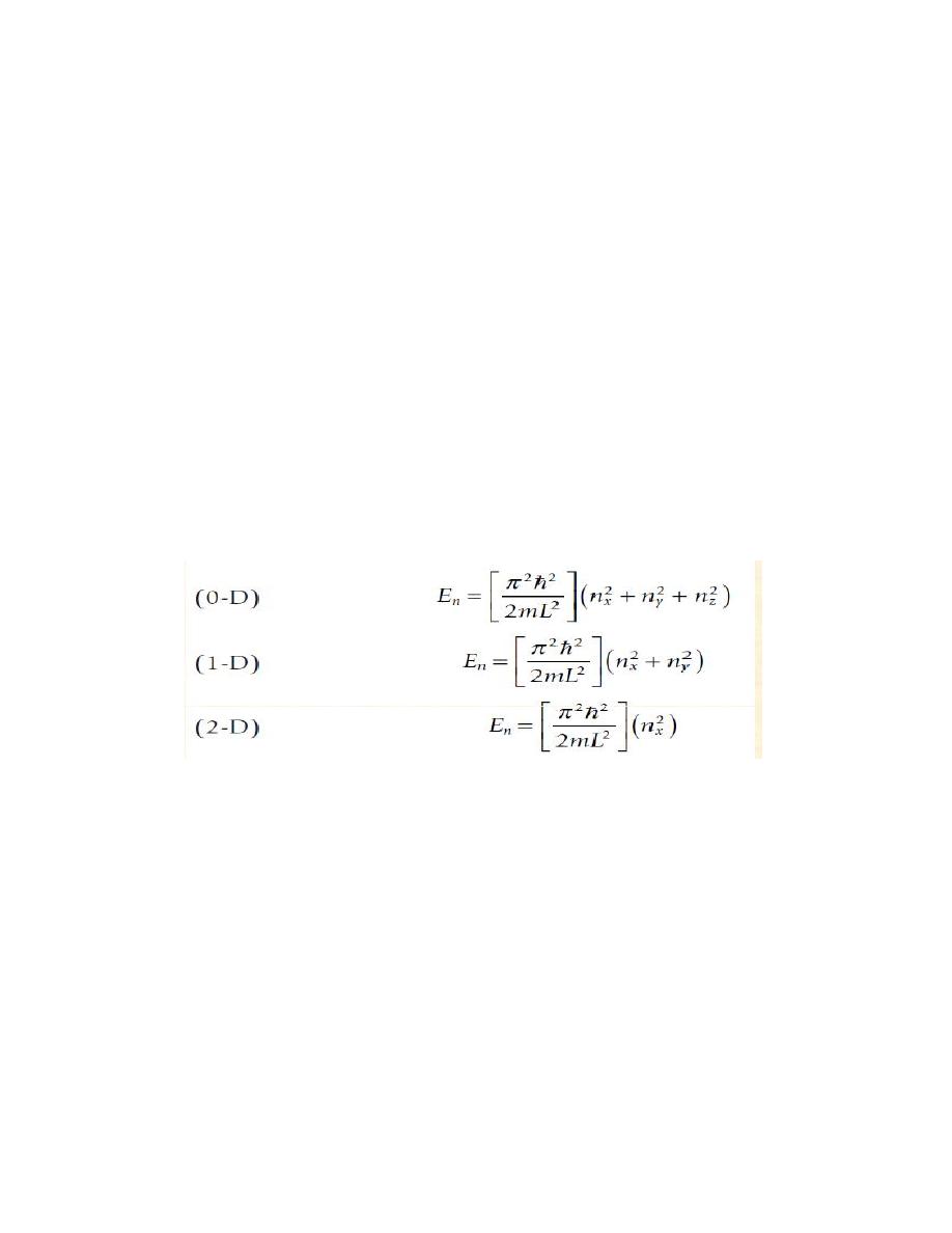
10-Electrons confinement
*For 0-D nanomaterials the electrons are fully confined.
* For 3-D nanomaterials the electrons are fully delocalized.
* In 1-D and 2-D nanomaterials, electron confinement and delocalization
coexist.
* The effect of confinement on the resulting energy states can 20
be calculated by quantum mechanics, as the “particle in the box”
problem. An electron is considered to exist inside of an infinitely deep
potential well (region of negative energies), from which it cannot escape
and is confined by the dimensions of the nanostructure.
11-Energies
where h_ _ h/2_, h is Planck’s constant, m is the mass of the electron, L is
the width(confinement) of the infinitely deep potential well, and nx, ny,
and nz are the principal quantum numbers in the three dimensions x, y,
and z.
The smaller the dimensions of the nanostructure (smaller L), the wider is
the separation between the energy levels, leading to a spectrum of
discreet energies.
What’s different at the nanoscale?
Each of the different sized arrangement of gold atoms absorbs and
reflects light differently based on its energy levels, which are determined
by size and bonding arrangement. This is true for many materials when
the particles have a size that is less than 100 nanometers in at least one
dimension.
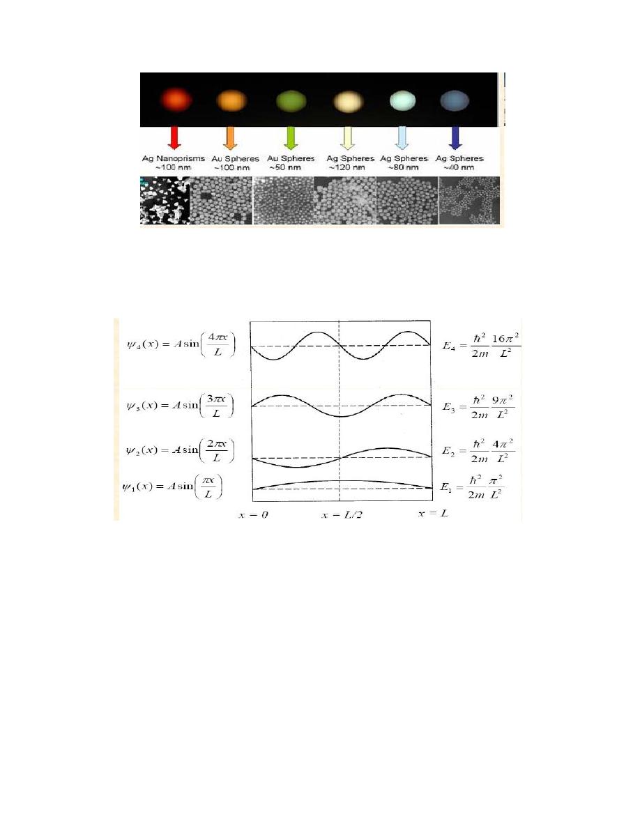
11-1Energy levels in infinite quantum well
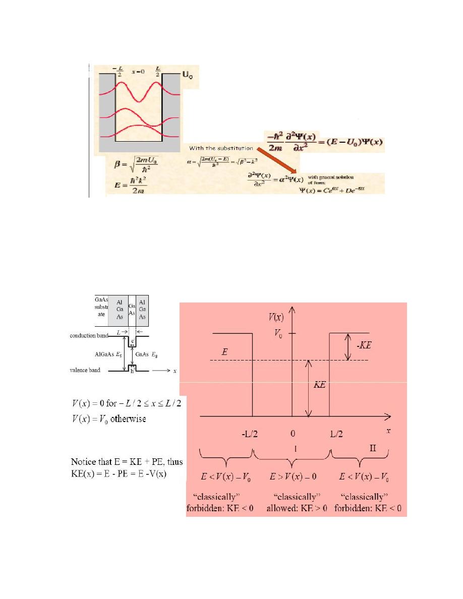
11-2The finite potential well
For the finite potential well, the solution to the Schrodinger equation
gives a wavefunction with an exponentially decaying penetration into the
classically forbidden region. Confining a particle to a smaller space
requires a larger confinement energy. Since the wave function penetration
effectively "enlarges the box", the finite well energy levels are lower than
those for the infinite well. The solution for -L/2 < x < L/2 and elsewhere
must satisfy the equation .
11-3Comparison of Infinite and Finite Potential Wells
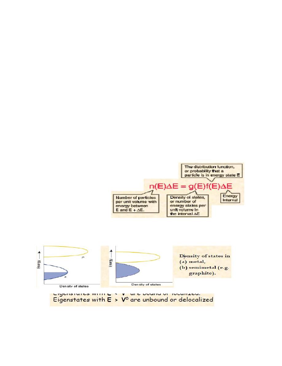
11-4Electron energy density
The behavior of electrons in solids depends upon the distribution of
energy among the electrons:
This distribution determines the probability that a given energy state will
be occupied, but must be multiplied by the density of states function to
weight the probability by the number of states available at a given energy.

Lecture 3
(nano
)
3 - Properties of Nanomaterials
Nanomaterials have the structural features in between of those of
atoms and the bulk materials. While most microstructured materials have
similar properties to the corresponding bulk materials, the properties of
materials with nanometer dimensions are significantly different from
those of atoms and bulks materials. This is mainly due to the
nanometer size of the materials which render them:
(i) large fraction of surface atoms;
(ii)high surface energy;
(iii) spatial confinement;
(iv) reduced imperfections,
which do not exist in the corresponding bulk materials. Due to their small
dimensions, nanomaterials have extremely large surface area to volume
ratio, which makes a large to be the surface or interfacial atoms, resulting
in more “surface” dependent material properties. Especially when the
sizes of nanomaterials are comparable to length, the entire material will
be affected by the surface properties of nanomaterials. This in turn may
enhance or modify the properties of the bulk materials.For example,
metallic nanoparticles can be used as very active catalysts. Chemical
sensors from nanoparticles and nanowires enhanced the sensitivity and
sensor selectivity. The nanometer feature sizes of nanomaterials also have
spatial confinement effect on the materials, which bring the quantum
effects.The energy band structure and charge carrier density in the
materials can be modified quite differently from their bulk and in turn
will modify the electronic and optical properties of the materials. For

example, lasers and light emitting diodes (LED) from both of the
quantum dots and quantum wires are very promising in the future
optoelections. High density information storage using quantum dot
devices is also a fast developing area. Reduced imperfections are also an
important factor in determination of the properties of the nanomaterials.
Nanosturctures and Nanomaterials favors of a selfpurification process in
that the impurities and intrinsic material defects will move to near
the surface upon thermal annealing. This increased materials perfection
affects the properties of nanomaterials. For example, the chemical
stability for certain nanomaterials may be enhanced, the mechanical
properties of nanomaterials will be better than the bulk materials. The
superior mechanical properties of carbon nanotubes are well known. Due
to their nanometer size, nanomaterials are already known to have many
novel properties. Many novel applications of the nanomaterials rose from
these novel properties have also been proposed. characteristics, and other
variables including doping and interaction with the surrounding
environment or other nanostructures. Likewise, shape can have dramatic
influence on optical properties of metal nanostructures.
Fig. () xemplifies
the difference in the optical properties of metal and semiconductor
nanoparticles. With the CdSe semiconductor nanoparticles, a simple
change in size alters the optical properties of the
3-1 Mechanical properties
“Mechanical Properties of Nanoparticles” deals with bulk metallic
and ceramic materials, influence of porosity, influence of grain size,
superplasticity, filled polymer composites, particle-filled polymers,
polymer-based nanocomposites filled with platelets, carbon nanotube-
based composites. The discussion of mechanical properties of
anomaterials is, in to some extent, only of quite basic interest, the reason
being that it is problematic to produce macroscopic bodies with a high

density and a grain size in the range of less than 100 nm. However, two
materials, neither of which is produced by pressing and sintering,
have attracted much greater interest as they will undoubtedly achieve
industrial importance.
These materials are polymers which contain nanoparticles or
nanotubes to improve their mechanical behaviors, and severely plastic-
deformed metals, which exhibit astonishing properties. However, because
of their larger grain size, the latter are generally not accepted as
nanomaterials. Experimental studies on the mechanical properties of bulk
nanomaterials are generally impaired by major experimental problems in
producing specimens with exactly defined grain sizes and porosities.
Therefore, model calculations Book title 1.25 and molecular dynamic
studies are of major importance for an understanding of the
mechanical properties of these materials.
Filling polymers with nanoparticles or nanorods and nanotubes,
respectively, leads to significant improvements in their mechanical
properties. Such improvements depend heavily on the type of the filler
and the way in which the filling is conducted. The latter point is of
special importance, as any specific advantages of a nanoparticulate filler
may be lost if the filler forms aggregates, thereby mimicking the large
particles. Particulatefilled polymer-based nanocomposites exhibit a broad
range of failure strengths and strains. This depends on the shape of the
filler, particles or platelets, and on the degree of agglomeration. In this
class of material, polymers filled with silicate platelets exhibit the
best mechanical properties and are of the greatest economic relevance.
The larger the particles of the filler or agglomerates, the poorer are the
properties obtained. Although, potentially, the best composites are those
filled with nanofibers or nanotubes, experience teaches that sometimes
such composites have the least ductility. On the other hand, by
using carbon nanotubes it is possible to produce composite fibers with
extremely high strength and strain at rupture. Among the most exciting
nanocomposites are the polymerceramic nanocomposites, where the
ceramic phase is platelet-shaped.
This type of composite is preferred in nature, and is found in the
structure of bones, where it consists of crystallized mineral platelets of a
few nanometers thickness that are bound together with collagen as the
matrix. Composites consisting of a polymer matrix and defoliated
phyllosilicates exhibit excellent mechanical and thermal properties.
3-2
Optical properties
One of the most fascinating and useful aspects of nanomaterials is
their optical properties.Applications based on optical properties of
nanomaterials include optical detector, laser,sensor, imaging, phosphor,
display,
solar
cell,
photocatalysis,
photoelectrochemistry
and
biomedicine.The optical properties of nanomaterials depend on
parameters such as feature size,shape, surface
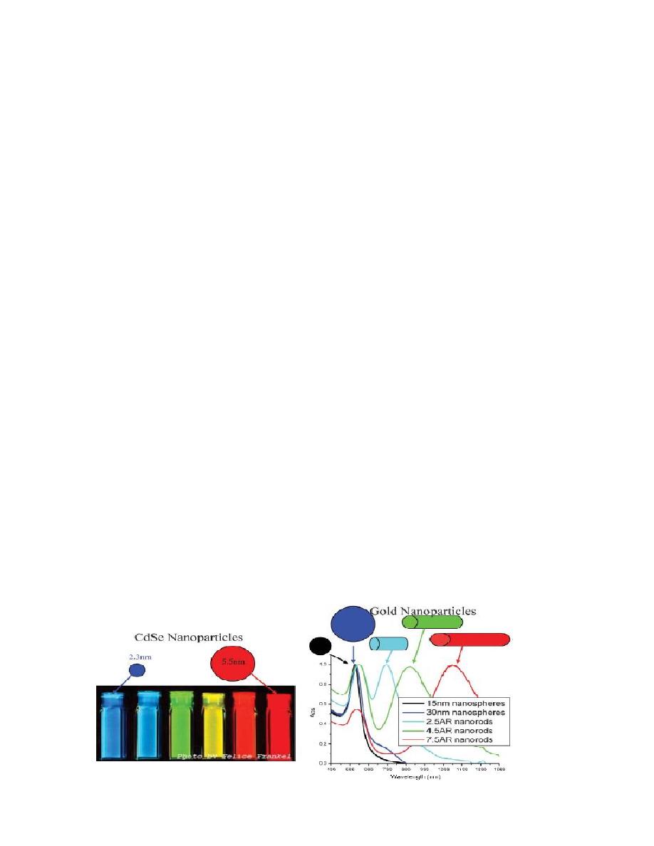
nanoparticles. When metal
nanoparticles are enlarged, their optical properties change only slightly as
observed for the different samples of gold nanospheres in fig.
().However, when an anisotropy is added to the nanoparticle, such as
growth of nanorods,the optical properties of the nanoparticles change
dramatically.
Fig.3-2
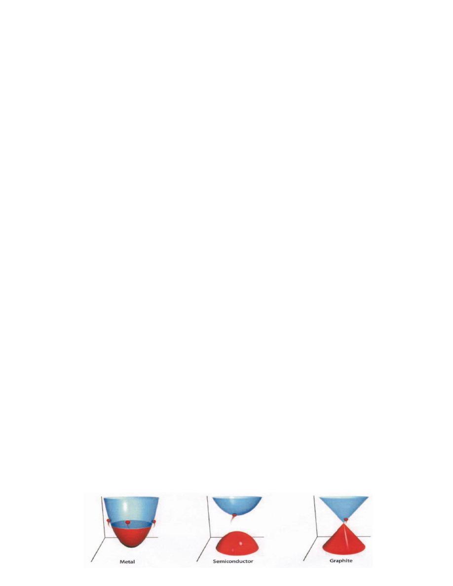
Fig. 4-1 Fluorescence emission of (CdSe) ZnS quantum dots of various
sizes and absorption spectra of various sizes and shapes of gold
nanoparticles .
3-3Electrical properties
Electrical Properties of Nanoparticles” discuss about fundamentals
of electrical conductivity in nanotubes and nanorods, carbon nanotubes,
photoconductivity of nanorods, electrical conductivity of anocomposites.
One interesting method which can be used to demonstrate the steps in
conductance is the mechanical thinning of a nanowire and measurement
of the electrical current at a constant applied voltage. The important
point here is that, with decreasing diameter of the wire, the number of
electron wave modes contributing to the electrical conductivity is
becoming increasingly smaller by well-defined quantized steps.
In electrically conducting carbon nanotubes, only one electron wave
mode is observed which transport the electrical current. As the lengths
and orientations of the carbon nanotubes are different, they touch the
surface of the mercury at different times,which provides two sets of
information:
(i) the influence of carbon nanotube length on 1.24 Introduction to
Nanomaterials the resistance; and
(ii) the resistances of the different nanotubes. As the nanotubes have
different lengths, then with increasing protrusion of the fiber bundle an
increasing number of carbon nanotubes will touch the surface of the
mercury droplet and contribute to the electrical current transport.
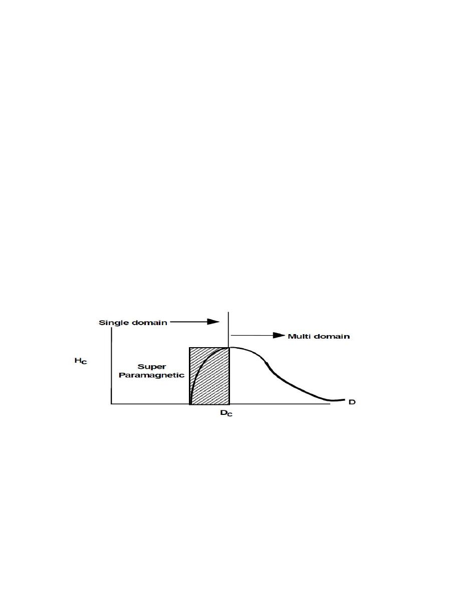
Fig. 4-2 Electrical behavior of naotubes.
3 – 4 Magnetic properties
Bulk gold and Pt are non-magnetic, but at the nano size they are
magnetic. Surface atoms are not only different to bulk atoms, but they can
also be modified by interaction with other chemical species, that is, by
capping the nanoparticles. This phenomenon opens the possibility to
modify the physical properties of the nanoparticles by capping them with
appropriate molecules. Actually, it should be possible that non-
ferromagnetic bulk materials exhibit ferromagnetic-like behavior when
prepared in nano range. One can obtain magnetic nanoparticles of Pd, Pt
and the surprising case of Au (that is diamagnetic in bulk) from non-
magnetic bulk materials. In the case of Pt and Pd, the ferromagnetism
arises from the structural changes associated with size effects
Fig. 4-3 Magnetic properties of nanostrucutred materials.
However, gold nanoparticles become ferromagnetic when they are
capped withappropriate molecules: the charge localized at the particle
surface gives rise toferromagnetic-like behavior. Surface and the core of
Au nanoparticles with 2 nm in diameter show ferromagnetic and
paramagnetic character, respectively. The large spin-orbit coupling of
these noble metals can yield to a large anisotropy and therefore exhibit
high ordering temperatures. More surprisingly, permanent magnetism
was observed up to room temperature for thiol-capped Au nanoparticles.
For nanoparticles with sizes below 2 nm the localized carriers are in the
5d band. Bulk Au has an extremely low density of states and becomes
diamagnetic, as is also the case for bare Au nanoparticles.
This observation suggested that modification of the d band structure
by chemical bonding can induce ferromagnetic like character in metallic
clusters.
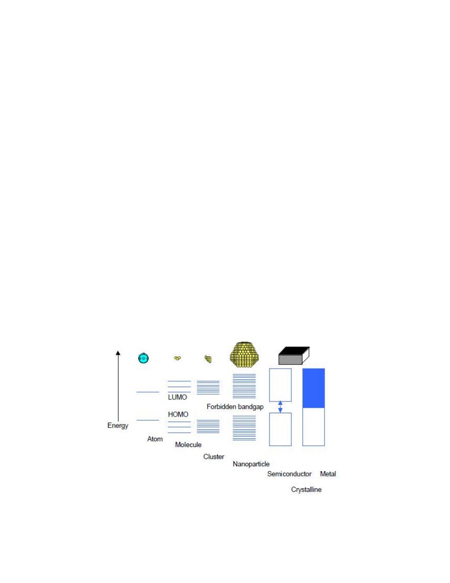
ELECTRONIC AND OPTICAL PROPERTIES OF
NANOMATERIALS
7.1 Introduction

Figure 7-1: Size quantization effect. Electronic state transition from bulk
metal/semiconductor to small cluster.
Nanocrystalline particles represent a state of matter in the transition
region between bulk solid and single molecule. As a consequence, their
physical and chemical properties gradually change from solid state to
molecular behaviour with decreasing particle size. The reasons for this
behaviour can be summarised as two basic phenomena.
First, as we have already discussed, owing to their small dimensions,
the surface-to-volume ratio increases, and the number of surface atoms
may be similar to or higher than those located in the crystalline lattice
core, and the surface properties are no longer negligible. When no other
molecules are adsorbed onto the nanocrystallites, the surface atoms are
highly unsaturated and their electronic contribution to the behaviour of
the particles is totally different from that of the inner atoms. These effects
may be even more marked when the surface atoms are ligated. This leads
to different mechanical and electronic transport properties,
which account for the catalytic properties of the nanocrystalline particles.
The second phenomenon, which only occurs in metal and semiconductor
nanoparticles, is totally an electronic effect. The band structure gradually
evolves with increasing particle size, i. e., molecular orbital convert into
delocalised band states. Figure above, shows the size quantization effect
responsible for the transition between a bulk metal or semiconductor, and
cluster species. In a metal, the quasicontinuous
density of states in the valence and the conduction bands splits into
discrete electronic levels, the spacing between these levels and the band
gap increasing with decreasing particle size.
In the case of semiconductors, the phenomenon is slightly
different, since a band gap already exists in the bulk state. However, this
band gap also increases when the particle size is decreased and the energy

bands gradually convert into discrete molecular electronic levels. If the
particle size is less than the De Broglie wavelength of the electrons, the
charge carriers may be treated quantum mechanically as "particles in a
box", where the size of the box is given by the dimensions of the
crystallites. In semiconductors, the quantization effect that
enhances the optical gap is routinely observed for clusters ranging from 1
nm to almost 10 nm. Metal particles consisting of 50 to 100 atoms with a
diameter between 1 and 2 nm start to loose their metallic behaviour and
tend to become semiconductors. Particles that show this size quantization
effect are sometimes called Q-particles or quantum dots that we will
discuss later in this chapter.Certain particle sizes, determined by the so-
called magic numbers, are more frequently observed than others. This is
not only due to the thermodynamic stability of certain structures but is
also related to the kinetics of particle growth. In semiconductor
nanoparticles such as CdS, the growth of the initially formed smallest
particles with an agglomeration number k occurs by combination of the
particles. Thus, particles so formed would have the agglomeration
number of 2k, 3k and so on.lxx Metals have a cubic or hexagonal close-
packed structure consisting of one central atom, which is surrounded in
the first shell by 12 atoms, in the second shell by 42 atoms, or in principle
by 10n2+2 atoms in the nth shell For example, one of the

Lecture 3
(nano
)
Mechanical properties of nanocrystalline metals and
alloys
In this section, we review the principal mechanical properties of
nanocrystalline metals: yield stress, ductility, strain hardening, strain-rate
sensitivity and dynamic response, creep and fatigue. At the outset, it
should be emphasized that porosity is of utmost importance and can mask
and/or distort properties. The early ‘‘bottom-up’’ synthesis methods often
resulted in porosity and incomplete bonding among the grains.
Processing flaws like porosity are known to be detrimental to the
properties of nanocrystalline materials. Fig. 11
shows the Young_s
modulus as a function of porosity for nanocrystalline Pd and Cu as shown
by Weertman et al.This decrease in Young_s modulus with porosity is
well known and is indeed expressed in many mechanics simulations.
One of the equations is Wachtman and MacKenzie
E ¼ E0ً1 _ f1p f2p2 ق
where p is the porosity and f1 and f2 are equal to 1.9 and 0.9,
respectively. For relatively low porosity, p2 can be neglected and we
have, approximately E E0 ¼ 1 _ 1:9p. The yield
stress and tensile ductility are simultaneously affected.
Fig. 12
shows as
an illustration,
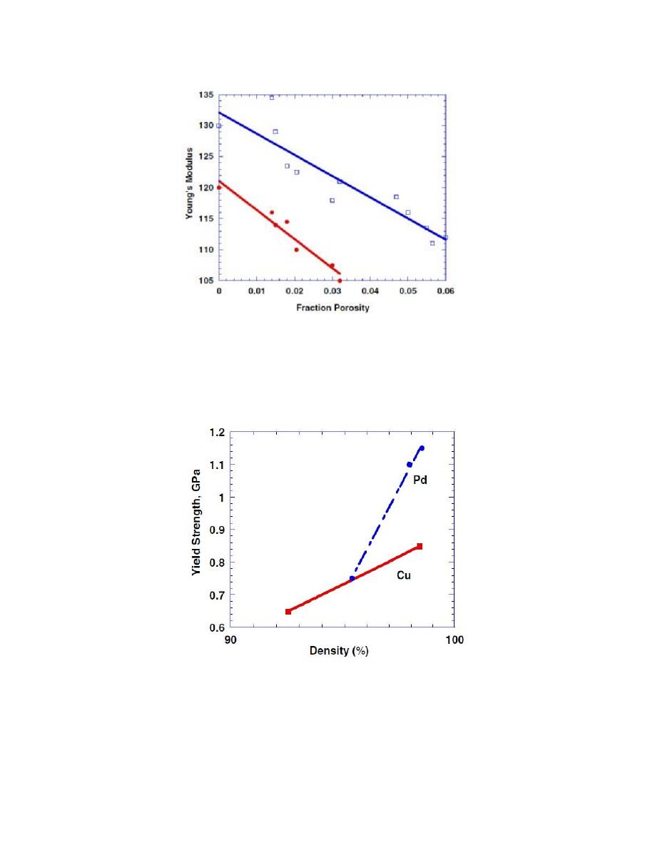
Fig. 11. Young_s modulus as a function of porosity for nanocrystalline
Pd and Cu.
Fig. 12. Compressive yield strength of Cu and Pd as a function of
consolidation density.

a plot of the yield stress as a function of density for Cu and Pd. The
decrease in strength isobvious. The existing pores provide initiation sites
for failure.
3-1- Yield strength
Grain size is known to have a significant effect on the mechanical
behavior of materials,in particular, on the yield stress. The dependence of
yield stress on grain size in metals iswell established in the conventional
polycrystalline range (micrometer and larger sized grains). Yield stress,
ry, for materials with grain size d, is found to follow the Hall–Petch
relation:
ry ¼ r0 kd_1=2 ً3 ق
where r0 is the friction stress and k is a constant. This is indeed an
approximation, and a more general formulation is to use a power
expression with exponent _n, where 0.3 6 n 6 0.7.
The mechanical properties of FCC metals with nano-range grain sizes
have been estimated from uniaxial tension/compression tests and micro-
or nano-indentation. Often micro-size tensile samples are used to avoid
the influence of imperfections e.g., voids
that might adversely influence the mechanical response of the material.
The compressive yield stresses of nanocrystalline Cu and Pd samples
synthesized by IGC are summarized in Table 2, and the plot is given in
Fig. 12. Weertman and coworkers observed that nanocrystalline Cu and
Pd samples were remarkably stronger than their coarse-grained
counterpart and this was a strong function of density. Their strain to
failure was also higher. Suryanarayana et al. reported compressive yield
strength of _500 MPa from their strongest nano Cu sample. Table 2 gives
the values of the Vickers hardness, Hv divided by 3, which approximates
to the yield strength if the work-hardening is not large. Unlike the case of
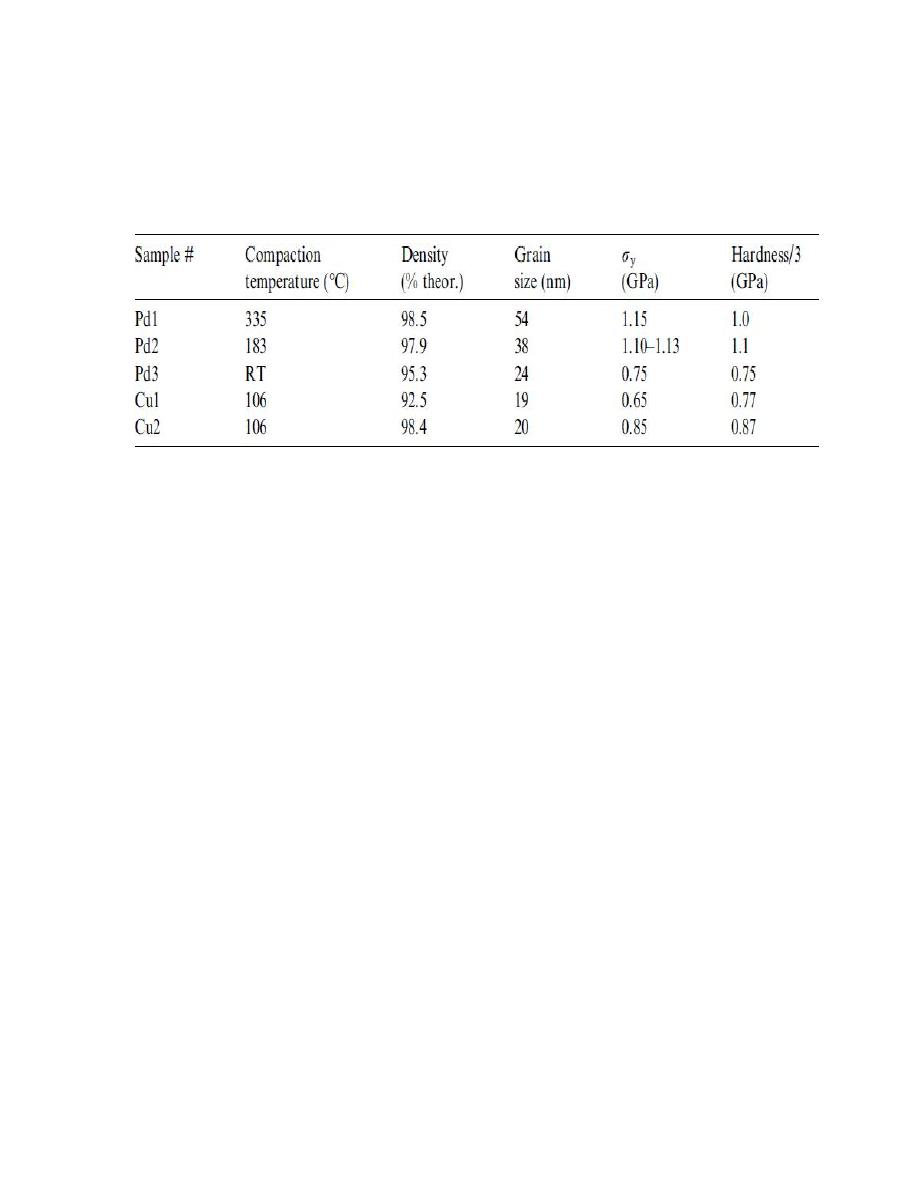
tensile yield strength, the compressive values of ry scale well with Hv/3.
Weertman et al. observed a large increase in hardness.
Table 2 Compressive yield strength of nanocrystalline Cu and Pd
synthesized by inert gas condensation method .
for the nanocrystalline Cu and Pd samples made by IGC as compared to
the annealed coarse-grained samples. It was difficult to separate the
magnitude of the strengthening effect of the small grain size from the
weakening effect due to the bulk sample defects which are inherent to the
IGC synthesis method (mainly pores).
3-2 Ductility
In the conventional grain size regime, usually a reduction in grain size
leads to an increase in ductility. Thus one should expect a ductility
increase as the grain size is reduced to nanoscale. However, the ductility
is small for most grain sizes <25 nm for metals that in the conventional
grain size have tensile ductilities of 40–60% elongation .
identified three major sources of limited ductility in nanocrystalline
materials, namely:
(1) artifacts from processing (2) tensile instability; (3) crack nucleation or
shear instability. It is difficult to process nanostructured materials free
from the artifacts that mask the inherent mechanical properties. As a

result, molecular dynamics simulation has been considered to be a
valuable tool in aiding our understanding of their deformation
mechanism . This is treated in greater detail in Section 9. The results of
the atomistic simulations have allowed several investigators to suggest
different plastic deformation mechanisms as a function of grain size .
There seems to be agreement in the existence of three regimes: (a) grain
size d > 1 lm regime in which unit dislocations and work hardening
control plasticity; (b) smallest grain size d < 10 nm regime, where limited
intragranular dislocation activity occurs and grain-boundary shear is
believed to be the mechanism of deformation. The intermediate grain size
regime (10 nm–1 lm) is less well understood. These mechanisms are
thought to affect ductility significantly.
Fig. 13(a) shows data on normalized yield strength (strength/strength of
conventional polycrystalline) versus percentage elongation in tension for
metals with grain sizes in the nanocrystalline range. There is a clear
decrease in ductility as strength is increased. By comparison, ultrafine
grained materials (100–500 nm), Fig. 13(b), exhibit increased yield
strength along with good ductility in comparison to nanograined
materials. varied the microstructure of nanostructured/ultrafine grain size
of Zn by changing the milling times. A very dramatic modulated cyclic
variation of hardness was observed as a function of milling time at liquid
nitrogen temperature. The sample cryomilled for 4 h exhibited an
optimum combination of strength and ductility. The grain size
distribution in this sample contained 30% volume fraction of grains larger
than 50 nm along with the smaller nano-scale grains. This optimum
microstructure, which exhibits
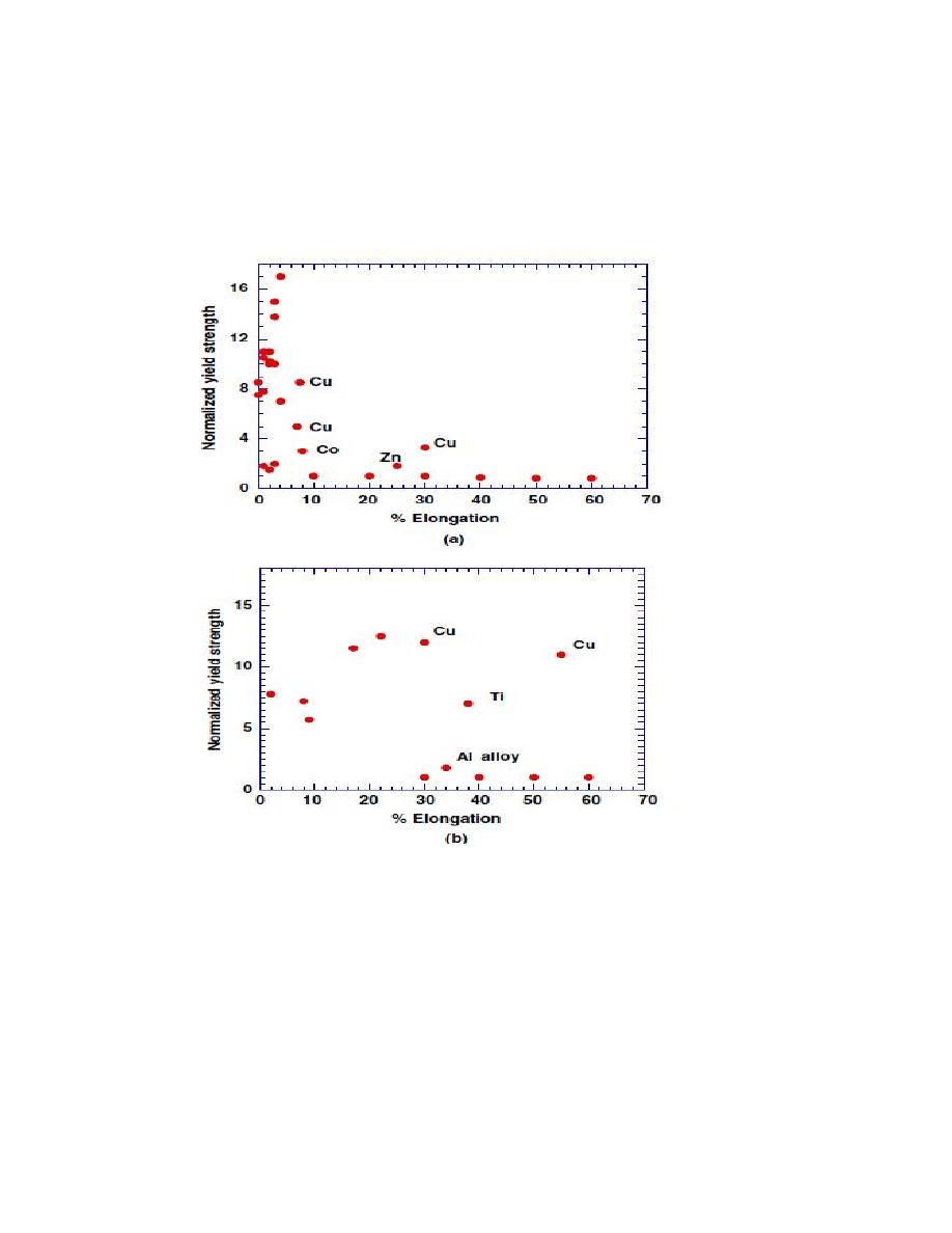
Fig. 13. (a) Compilation of yield stress versus % elongation showing the
reduced ductility of nanocrystalline metals
[96]
. (b) Compilation of yield
strength versus % elongation of various ultrafine grained metals

more strain hardening than samples milled for either shorter or longer
time, combined the strengthening from the reduced grain size along with
the strain hardening provided by dislocation activity in the larger grains.
This strain hardening, in turn, provided ductility. Thus, a bimodal grain
size distribution is a possible means to increase ductility.
Nonequilibrium grain boundaries have also been proposed as a
mechanism to enhance ductility. It has been argued that such boundaries
provide a large number of excess dislocations for slip and can even
enable grains to slide or rotate at room temperature, leading to a
significant increase in the strain hardening exponent. Another way of
increasing ductility is to decrease the strain rate in order for the specimen
to sustain more plastic strain prior to necking.
Fig. 13. (a) Compilation of yield stress versus % elongation showing the
reduced ductility of nanocrystalline metals. (b) Compilation of yield
strength versus % elongation of various ultrafine grained metals.
Fig. 14
(a) shows the expected ductility of metals as a function of a
normalized strength (strength in the conventional grain size domain). As
expected, as the strength increases, the ductility decreases. This defines
the grey region. However, there are five data points above this boundary.
They all apply to copper. Three factors contribute to and in fact determine
ductility: the work hardening, the strain rate sensitivity and thermal
softening. The increased ductility that is exhibited in some cases comes,
basically, from the inhibition of shear localization. The strain rate
sensitivity, m, can be expressed as:
m ¼
31=2kT
V ry
ً4 ق
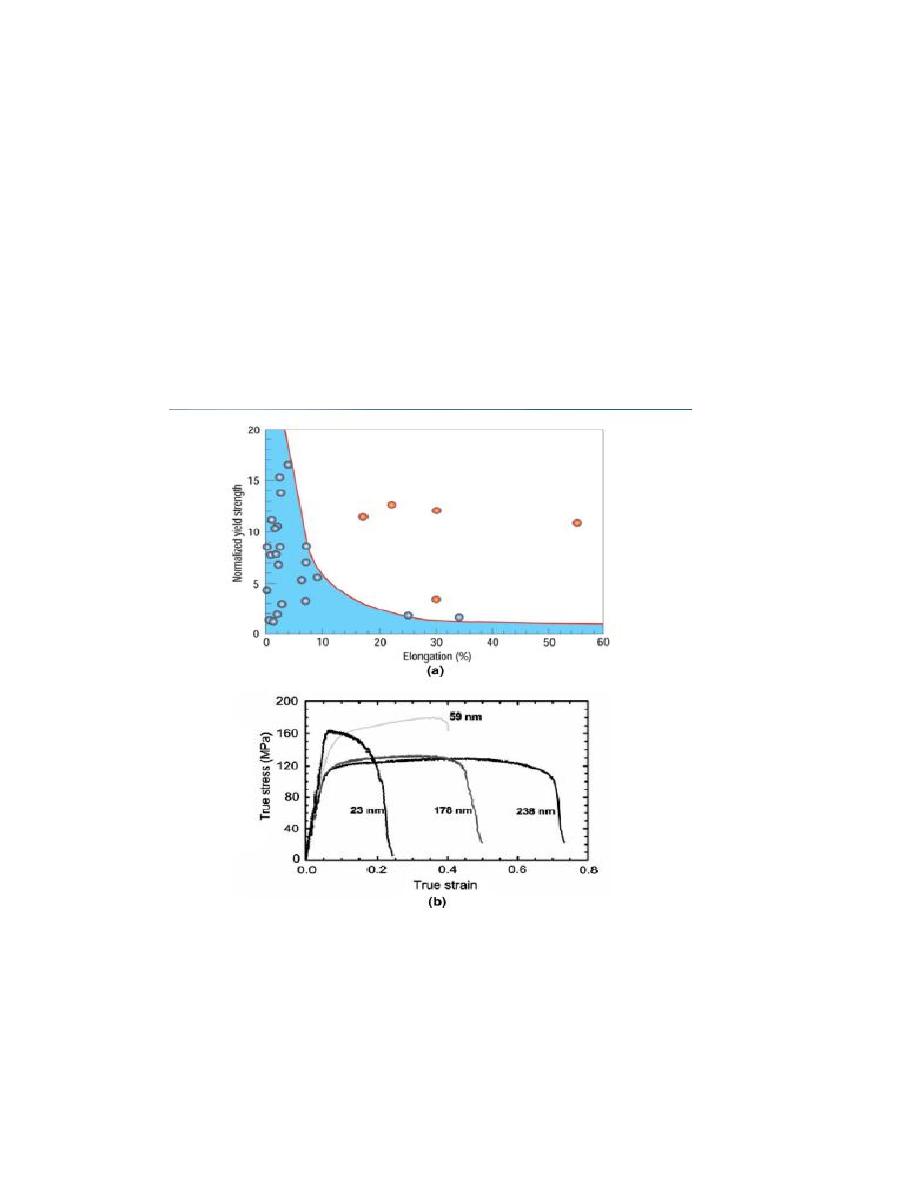
where V is the activation volume for plastic deformation (which is
directly related to the physical mechanism of deformation), T is the
temperature, and ry is the yield/flow stress. The higher strain-rate
sensitivity ًm ¼ o ln r=o ln _e or 1
ry
or
o ln _e قis indicative of a smaller activation volume, as pointed out by Lu
et al.
Fig. 14. (a) Increased ductility in the nanocrystalline regime as indicated
by experimental points in right-hand side of diagram; (b) reduction of
ductility as grain size is reduced for ball milled Zn tested at a constant
strain rate of 10_4–10_3 s_1 at room temperature

This, in turn, is connected to a change in the nanostructure (presence of
twins). Thus, ductility, strain rate sensitivity, and deformation
mechanisms are connected and it is possible, through the manipulation of
the nanostructure to increase ductility. were able to increase ductility of
their nanocrystalline metals by increasing significantly the density of
growth (annealing) twins. (b) shows the mechanical response of
nanocrystalline zinc samples with different grain sizes. There is a
significant drop in ductility as the grain size goes down from 238 nm to
23 nm. Zhang et al. suggested that the reduction of elongation with the
reduction of grain size could be an inherent property of nanocrystalline
materials given that there is no porosity and bonding was complete during
synthesis. Earlier results have shown that the mechanical properties of
nanocrystalline materials can be misinterpreted because of the lack of
attention to the details of the internal structure. As mentioned earlier,
contaminates and porosity are found to be extremely detrimental to
ductility

Lecture 4
(nano
)
4 Methods for creating nanostructures
There are many different ways of creating nanostructures: of course,
macromolecules or nanoparticles or buckyballs or nanotubes and so on
can be synthesized artificially for certain specific materials. They can also
be arranged by methods based on equilibrium or near-equilibrium
thermodynamics such as methods of self-organization and self-assembly
(sometimes also called bio-mimetic processes). Using these methods,
synthesized materials can be arranged into useful shapes so that finally
the material can be applied to a certain application.
4-1 Mechanical grinding
Mechanical attrition is a typical example of ‘top down’ method of
synthesis of nanomaterials, where the material is prepared not by cluster
assembly but by the structural decomposition of coarser-grained
structures as the result of severe plastic deformation. This has become a
popular method to make nanocrystalline materials because of its
simplicity, the relatively inexpensive equipment needed, and the
applicability to essentially the synthesis of all classes of materials. The
major advantage often quoted is the possibility for easily scaling up to
tonnage quantities of material for various applications. Similarly, the
serious problems that are usually cited are;
1. contamination from milling media and/or atmosphere, and
2. to consolidate the powder product without coarsening the
nanocrystalline microstructure. In fact, the contamination problem is
often given as a reason to dismiss the method, at least for some materials.
Here we will review the mechanisms presently believed responsible for

formation of nanocrystalline structures by mechanical attrition of single
phase powders, mechanical alloying of dissimilar powders, and
mechanical
crystallisation of amorphous materials. The two important problems of
contamination and Mechanical milling is typically achieved using high
energy shaker, planetary ball, or tumbler mills. The energy transferred to
the powder from refractory or steel balls depends on the rotational
(vibrational) speed, size and number of the balls, ratio of the ball to
powder mass, the time of milling and the milling atmosphere
.
Nanoparticles are produced by the shear action during grinding.
Milling in cryogenic liquids can greatly increase the brittleness of the
powders influencing the fracture process. As with any process that
produces fine particles, an adequate step to prevent oxidation is
necessary. Hence this process is very restrictive for the production of
non-oxide materials since then it requires that the milling take place in
an inert atmosphere and that the powder particles be handled in an
appropriate vacuum system or glove box. This method of synthesis is
suitable for producing amorphous or nanocrystalline alloy particles,
elemental or compound powders. If the mechanical milling imparts
sufficient energy to the constituent powders a homogeneous alloy can be
formed. Based on the energy of the milling process and thermodynamic
properties of the constituents the alloy can be rendered amorphous by this
processing.
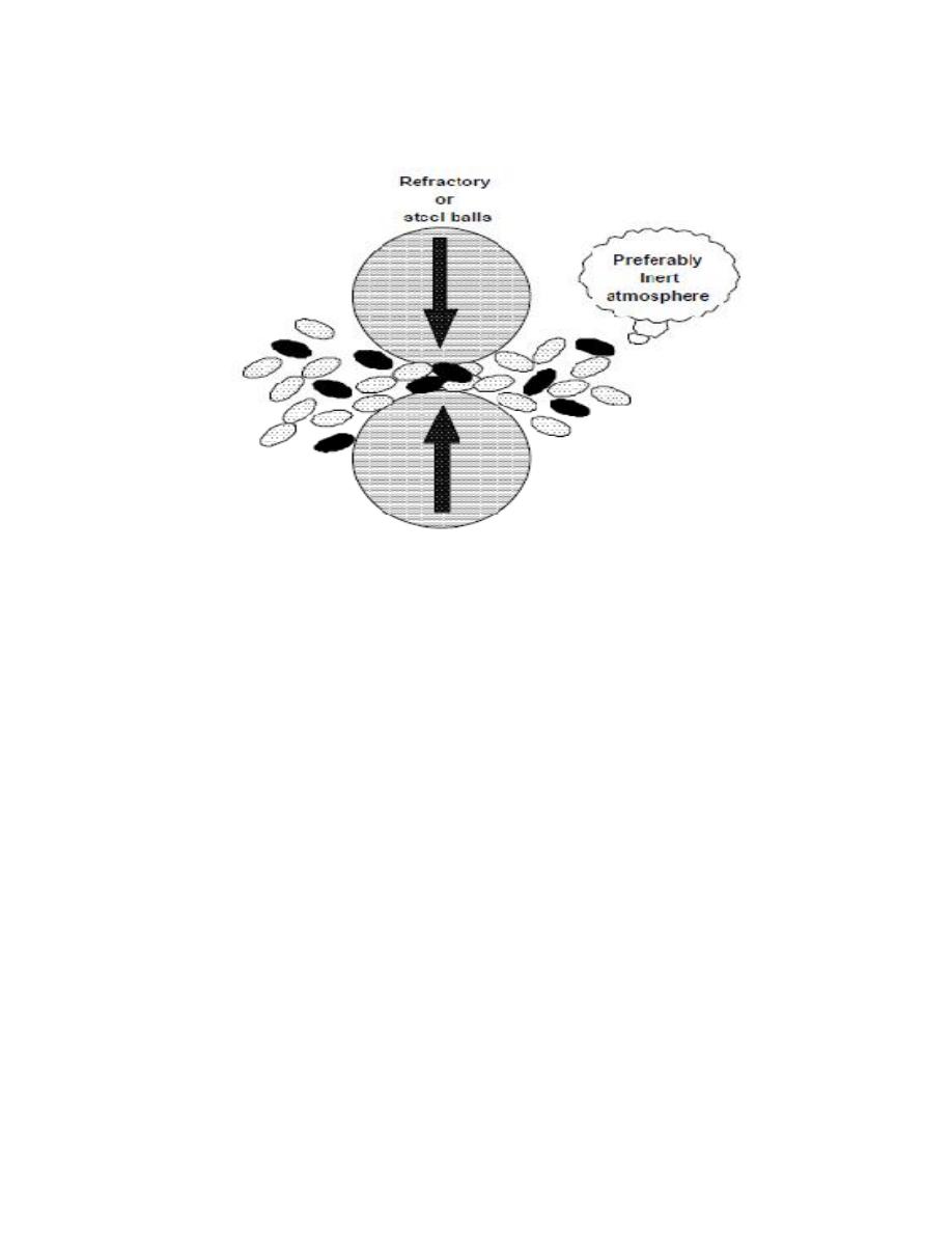
Fig. 6. Schematic representation of the principle of mechanical milling
4-2 Wet Chemical Synthesis of Nanomaterials
In principle we can classify the wet chemical synthesis of
nanomaterials into two broad groups:
1. The top down method: where single crystals are etched in an aqueous
solution for producing nanomaterials, For example, the synthesis of
porous silicon by electrochemical etching.
2. The bottom up method: consisting of sol-gel method, precipitation etc.
where materials containing the desired precursors are mixed in a
controlled fashion to form a colloidal solution.
4-2- 1 Sol-gel process
The sol-gel process, involves the evolution of inorganic networks
through the formation of a colloidal suspension (sol) and gelation of the
sol to form a network in a continuous liquid phase (gel). The precursors
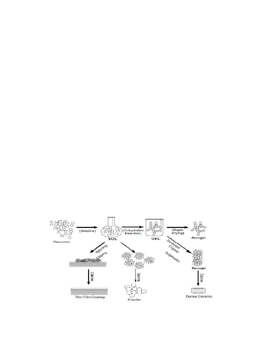
for synthesizing these colloids consist usually of a metal or metalloid
element surrounded by various reactive ligands. The starting material
is processed to form a dispersible oxide and forms a sol in contact with
water or dilute acid. Removal of the liquid from the sol yields the gel, and
the sol/gel transition controls the particle size and shape. Calcination of
the gel produces the oxide.
Sol-gel processing refers to the hydrolysis and condensation of
alkoxide-based precursors such as Si(OEt) 4 (tetraethyl orthosilicate, or
TEOS). The reactions involved in the sol-gel chemistry based on the
hydrolysis and condensation of metal alkoxides
M(OR)z can be described as follows:
MOR + H2O → MOH + ROH (hydrolysis)
MOH + ROM → M-O-M + ROH (condensation)
Sol-gel method of synthesizing nanomaterials is very popular amongst
chemists and is widely employed to prepare oxide materials. The sol-gel
process can be characterized by a series of distinct steps.
Fig. 7. Schematic representation of sol-gel process of synthesis of
nanomaterials.

1. Formation of different stable solutions of the alkoxide or solvated
metal precursor.
2. Gelation resulting from the formation of an oxide- or alcohol- bridged
network (the gel) by a polycondensation reaction that results in a
dramatic increase in the viscocity of the solution.
3. Aging of the gel (Syneresis), during which the polycondensation
reactions continue until the gel transforms into a solid mass, accompanied
by contraction of the gel network and expulsion of solvent from gel
pores. Ostwald ripening (also referred to as coarsening, is the
phenomenon by which smaller particles are consumed by larger particles
during the growth process) and phase transformations may occur
concurrently with syneresis. The aging process of gels can exceed 7 days
and is critical to the prevention of cracks in gels that have been
cast.
4. Drying of the gel, when water and other volatile liquids are removed
from the gel network. This process is complicated due to fundamental
changes in the structure of the gel. The drying process has itself been
broken into four distinct steps:
(i) the constant rate period, (ii) the critical point, (iii) the falling rate
period, (iv) the second falling rate period. If isolated by thermal
evaporation, the resulting monolith is termed a xerogel. If the solvent
(such as water) is extracted under supercritical or near super critical
conditions, the product is an aerogel.
5. Dehydration, during which surface- bound M-OH groups are removed,
there by stabilizing the gel against rehydration. This is normally achieved
by calcining the monolith at temperatures up to 8000C.
6. Densification and decomposition of the gels at high temperatures
(T>8000C). The pores of the gel network are collapsed, and remaining

organic species are volatilized. The typical steps that are involved in sol-
gel processing are shown in the schematic diagram below.
The interest in this synthesis method arises due to the possibility of
synthesizing nonmetallic inorganic materials like glasses, glass ceramics
or ceramic materials at very low temperatures compared to the high
temperature process required by melting glass or firing ceramics.
The major difficulties to overcome in developing a successful bottom-up
approach is controlling the growth of the particles and then stopping the
newly formed particles from agglomerating. Other technical issues are
ensuring the reactions are complete so that no unwanted reactant is left on
the product and completely removing any growth aids that may have been
used in the process. Also production rates of nano powders are very low
by this process. The main advantage is one can get monosized nano
particles by any bottom up approach.
4-3 Gas Phase synthesis of nanomaterials
The gas-phase synthesis methods are of increasing interest because
they allow elegant way to control process parameters in order to be able
to produce size, shape and chemical composition controlled
nanostructures. Before we discuss a few selected pathways for gas-phase
formation of nanomaterials, some general aspects of gas-phase synthesis
needs to be discussed. In conventional chemical vapour deposition
(CVD) synthesis, gaseous products either are allowed to react
homogeneously or heterogeneously depending on a particular application.
1. In homogeneous CVD, particles form in the gas phase and diffuse
towards a cold surface due to thermophoretic forces, and can either be
scrapped of from the cold surface to give nano-powders, or deposited
onto a substrate to yield what is called ‘particulate films’.
2. In heterogeneous CVD, the solid is formed on the substrate surface,
which catalyses the reaction and a dense film is formed.

In order to form nanomaterials several modified CVD methods have been
developed. Gas phase processes have inherent advantages, some of which
are noted here:
� An excellent control of size, shape, crystallinity and chemical
composition
� Highly pure materials can be obtained
� Multicomonent systems are relatively easy to form
� Easy control of the reaction mechanisms
Most of the synthesis routes are based on the production of small
clusters that can aggregate to form nano particles (condensation).
Condensation occurs only when the vapour is supersaturated and in these
processes homogeneous nucleation in the gas phase is utilised to form
particles. This can be achieved both by physical and chemical methods.
4-3-1 Furnace
The simplest fashion to produce nanoparticles is by heating the
desired material in a heatresistant crucible containing the desired
material. This method is appropriate only for materials that have a high
vapour pressure at the heated temperatures that can be as high as 2000°C.
Energy is normally introduced into the precursor by arc heating,
electronbeam heating or Joule heating. The atoms are evaporated into an
atmosphere, which is either inert (e.g. He) or reactive (so as to form a
compound). To carry out reactive synthesis, materials with very low
vapour pressure have to be fed into the furnace in the form of a suitable
precursor such as organometallics, which decompose in the furnace to
produce a condensable material. The hot atoms of the evaporated matter
lose energy by collision with the atoms of the cold gas and undergo
condensation into small clusters via homogeneous nucleation. In case a
compound is being synthesized, these precursors react in the gas phase
and form a compound with the material that is separately injected in the
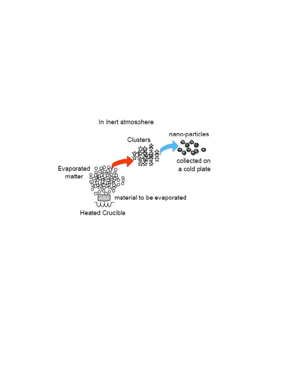
reaction chamber. The clusters would continue to grow if they remain in
the supersaturated region. To control their size, they need to be rapidly
removed from the supersaturated environment by a carrier gas. The
cluster size and its distribution are controlled by only three parameters:
1) the rate of evaporation (energy input),
2) the rate of condensation (energy removal), and
3) the rate of gas flow (cluster removal).
Fig. 8. Schematic representation of gas phase process of synthesis of
single phase nanomaterials from a heated crucible.
Because of its inherent simplicity, it is possible to scale up this process
from laboratory (mg/day) to industrial scales (tons/day).
4-3-2 Flame assisted ultrasonic spray pyrolysis
In this process, precusrsors are nebulized and then unwanted
components are burnt in a flame to get the required material, eg. ZrO2
has been obtained by this method from a precursor of Zr(CH3 CH2
CH2O)4. Flame hydrolysis that is a variant of this process is
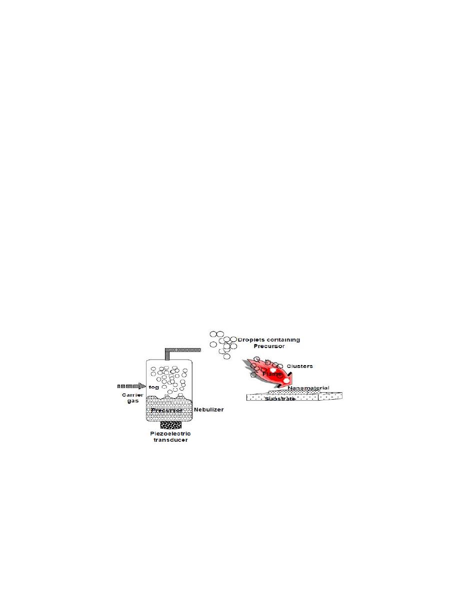
used for the manufacture of fused silica. In the process, silicon
tetrachloride is heated in an oxy-hydrogen flame to give a highly
dispersed silica. The resulting white amorphous powder consists of
spherical particles with sizes in the range 7-40 nm. The combustion
flame synthesis, in which the burning of a gas mixture, e.g. acetylene and
oxygen or hydrogen and oxygen, supplies the energy to initiate the
pyrolysis of precursor compounds, is widely used for the industrial
production of powders in large quantities, such as carbon black, fumed
silica and titanium dioxide. However, since the gas pressure
during the reaction is high, highly agglomerated powders are produced
which is disadvantageous for subsequent processing. The basic idea of
low pressure combustion flame synthesis is to extend the pressure range
to the pressures used in gas phase synthesis and thus to reduce or avoid
the agglomeration. Low pressure flames have been extensively used by
aerosol scientists to study particle formation in the flame.
Fig. 9. Flame assisted ultrasonic spray pyrolysis.
A key for the formation of nanoparticles with narrow size
distributions is the exact control of the flame in order to obtain a flat
flame front. Under these conditions the thermal history, i.e. time and
temperature, of each particle formed is identical and narrow

distributions result. However, due to the oxidative atmosphere in the
flame, this synthesis process is limited to the formation of oxides in the
reactor zone.
4-3-3 Gas Condensation Processing (GPC)
In this technique, a metallic or inorganic material, e.g. a suboxide,
is vaporised using thermal evaporation sources such as crucibles, electron
beam evaporation devices or sputtering sources in an atmosphere of 1-50
mbar He (or another inert gas like Ar, Ne, Kr). Cluster form in the
vicinity of the source by homogenous nucleation in the gas phase
and grow by coalescence and incorporation of atoms from the gas phase.
Fig. 10. Schematic representation of typical set-up for gas condensation
synthesis of nanomaterials followed by consolidation in a mechanical
press or collection in an appropriate solvent media.
The cluster or particle size depends critically on the residence time of
the particles in the growth system and can be influenced by the gas
pressure, the kind of inert gas, i.e. He, Ar or Kr, and on the evaporation
rate/vapour pressure of the evaporating material. With increasing gas
pressure, vapour pressure and mass of the inert gas used the average
particle size of the nanoparticles increases. Lognormal size distributions
have been found experimentally and have been explained theoretically by
the growth mechanisms of the particles. Even in more complex processes
such as the low pressure combustion flame synthesis where a number of
chemical reactions are involved the size distributions are determined to be
lognormal. Originally, a rotating cylindrical device cooled with liquid
nitrogen was employed for the particle collection: the nanoparticles in the
size range from 2-50 nm are extracted from the gas flow by
thermophoretic forces and deposited loosely on the surface of the
collection device as a powder of low density and no agglomeration.
Subsequenly, the nanoparticles are removed from the surface of the

cylinder by means of a scraper in the form of a metallic plate. In addition
to this cold finger device several techniques known from aerosol science
have now been implemented for the use in gas condensation
systems such as corona discharge, etc. These methods allow for the
continuous operation of the collection device and are better suited for
larger scale synthesis of nanopowders.
However, these methods can only be used in a system designed for gas
flow, i.e. a dynamic vacuum is generated by means of both continuous
pumping and gas inlet via mass flow controller. A major advantage over
convectional gas flow is the improved control of the particle sizes. It has
been found that the particle size distributions in gas flow systems, which
are also lognormal, are shifted towards smaller average values with
an appreciable reduction of the standard deviation of the distribution.
Depending on the flow rate of the He-gas, particle sizes are reduced by
80% and standard deviations by 18%.
The synthesis of nanocrystalline pure metals is relatively
straightforward as long as evaporation can be done from refractory metal
crucibles (W, Ta or Mo). If metals with high melting points or metals
which react with the crucibles, are to be prepared,sputtering, i.e. for W
and Zr, or laser or electron beam evaporation has to be used.
Synthesis of alloys or intermetallic compounds by thermal evaporation
can only be done in the exceptional cases that the vapour pressures of the
elements are similar. As an alternative, sputtering from an alloy or mixed
target can be employed. Composite materials such as Cu/Bi or W/Ga
have been synthesised by simultaneous evaporation from two separate
crucibles onto a rotating collection device. It has been found that
excellent intermixing on the scale of the particle size can be obtained.
However, control of the composition of the elements has been difficult
and reproducibility is poor. Nanocrystalline oxide powders are formed by

controlled postoxidation of primary nanoparticles of a pure metal (e.g. Ti
to TiO2) or a suboxide (e.g. ZrO to ZrO2). Although the gas
condensation method including the variations have been widely employed
to prepared a variety of metallic and ceramic materials, quantities
have so far been limited to a laboratory scale. The quantities of metals are
below 1 g/day, while quantities of oxides can be as high as 20 g/day for
simple oxides such as CeO2 or ZrO2. These quantities are sufficient for
materials testing but not for industrial production. However, it should be
mentioned that the scale-up of the gas condensation method for industrial
production of nanocrystalline oxides by a company called nanophase
technologies has been successful.
4-3-4 Chemical Vapour Condensation (CVC)
As shown schematically in Figure, the evaporative source used in
GPC is replaced by a hot wall reactor in the Chemical Vapour
Condensation or the CVC process. Depending on the processing
parameters nucleation of nanoparticles is observed during chemical
vapour deposition (CVC) of thin films and poses a major problem in
obtaining good film qualities. The original idea of the novel CVC process
which is schematically shown below where, it was intended to adjust the
parameter field during the synthesis in order to suppress film formation
and enhance homogeneous nucleation of particles in the gas flow. It is
readily found that the residence time of the precursor in the reactor
determines if films or particles are formed. In a certain range of residence
time both particle and formation can be obtained.
Adjusting the residence time of the precursor molecules by changing the
gas flow rate, the pressure difference between the precursor delivery
system and the main chamber occurs. Then the temperature of the hot
wall reactor results in the fertile production of nanosized particles of
metals and ceramics instead of thin films as in CVD processing. In

the simplest form a metal organic precursor is introduced into the hot
zone of the reactor using mass flow controller. Besides the increased
quantities in this continuous processcompared to GPC has been
demonstrated that a wider range of ceramics including nitrides and
carbides can be synthesised. Additionally, more complex oxides such as
BaTiO3 or composite structures can be formed as well. Appropriate
precursor compounds can be readily found in the CVD literature. The
extension to production of nanoparticles requires the determination of a
modified parameter field in order to promote particle formation instead of
film formation. In addition to the formation of single phase nanoparticles
by CVC of a single precursor the reactor allows the synthesis of
1. mixtures of nanoparticles of two phases or doped nanoparticles by
supplying two precursors at the front end of the reactor, and
2. coated nanoparticles, i.e., n-ZrO2 coated with n-Al2O3 or vice
versa, by supplying a second precursor at a second stage of the reactor. In
this case nanoparticles which have been formed by homogeneous
nucleation are coated by heterogeneous nucleation in a second stage of
the reactor.
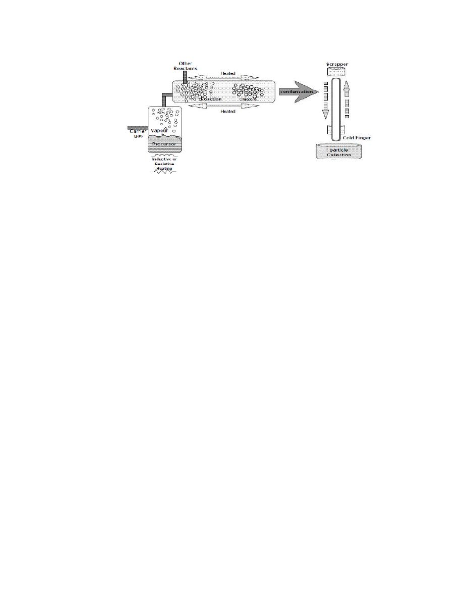
Fig. 11. A schematic of a typical CVC reactor.
Because CVC processing is continuous, the production capabilities
are much larger than in GPC processing. Quantities in excess of 20 g/hr
have been readily produced with a small scale laboratory reactor. A
further expansion can be envisaged by simply enlarging the diameter of
the hot wall reactor and the mass flow through the reactor.
4-4 Sputtered Plasma Processing:
In this method is yet again a variation of the gas-condensation
method excepting the fact that the source material is a sputtering target
and this target is sputtered using rare gases and the constituents are
allowed to agglomerate to produce nanomaterial. Both dc (direct
current) and rf (radio-frequency) sputtering has been used to synthesize
nanoparticles.
Again reactive sputtering or multitarget sputtering has been used to
make alloys and/or oxides, carbides, nitrides of materials. This method is
specifically suitable for the preparation of ultrapure and non-
agglomerated nanoparticles of metal.

5-6 Microwave Plasma Processing
This technique is similar to the previously discussed CVC
method but employs plasma instead of high temperature for
decomposition of the metal organic precursors. The method uses
microwave plasma in a 50 mm diameter reaction vessel made of quartz
placed in a cavity connected to a microwave generator. A precursor such
as a chloride compound is introduced into the front end of the reactor.
Generally, the microwave cavity is designed as a single mode cavity
using the TE10 mode in a WR975 waveguide with a frequency of 0.915
GHz. The major advantage of the plasma assisted pyrolysis in contrast to
the thermal activation is the low temperature reaction which reduces the
tendency for agglomeration of the primary particles. This is also true in
the case of plasma-CVD processes. Additionally, it has been shown that
by introducing another precursor into a second reaction zone of the
tubular reactor, e.g. by splitting the microwave guide tubes, the primary
particles can be coated with a second phase. For example, it has been
demonstrated that ZrO2 nanoparticles can be coated by Al2O3. In
this case the inner ZrO2 core is crystalline, while the Al2O3 coating is
amorphous. The reaction sequence can be reversed with the result that an
amorphous Al2O3 core is coated with crystalline ZrO2. While the
formation of the primary particles occurs by homogeneous nucleation, it
can be easily estimated using gas reaction kinetics that the coating on the
primary particles grows heterogeneously and that homogeneous
nucleation of nanoparticles originating from the second compound has a
very low probability. A schematic representation of the particle growth in
plasma’s is given below:
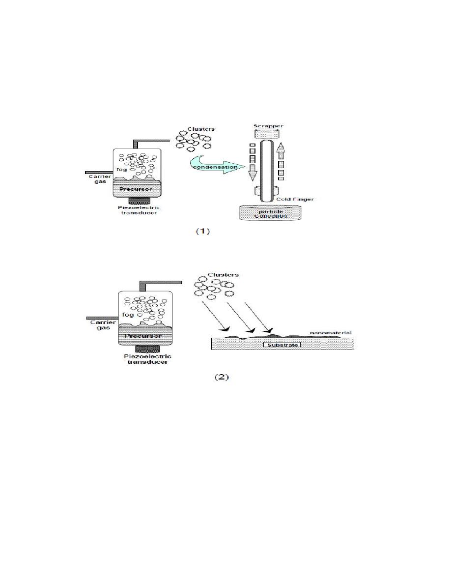
5-7 Particle precipitation aided CVD:
Fig. 12. Schematic representation of (1) nanoparticle, and (2) particulate
film formation .
In another variation of this process, colloidal clusters of materials
are used to prepare nanoparticles. The CVD reaction conditions are so set
that particles form by condensation in the gas phase and collect onto a
substrate, which is kept under a different condition that allows
heterogeneous nucleation. By this method both nanoparticles and
particulate films can be prepared. An example of this method has been

used to form nanomaterials eg. SnO2, by a method called pyrosol
deposition process, where clusters of tin hydroxide are transformed into
small aerosol droplets, following which they are reacted onto a
heated glass substrate.
5-8 Laser ablation
Laser ablation has been extensively used for the preparation of
nanoparticles and particulate films. In this process a laser beam is used as
the primary excitation source of ablation for generating clusters directly
from a solid sample in a wide variety of applications. The small
dimensions of the particles and the possibility to form thick films
make this method quite an efficient tool for the production of ceramic
particles and coatings and also an ablation source for analytical
applications such as the coupling to induced coupled plasma emission
spectrometry, ICP, the formation of the nanoparticles has been explained
following a liquefaction process which generates an aerosol, followed
by the cooling/solidification of the droplets which results in the formation
of fog. The general dynamics of both the aerosol and the fog favours the
aggregation process and micrometer-sized fractal-like particles are
formed. The laser spark atomizer can be used
to produce highly mesoporous thick films and the porosity can be
modified by the carrier gas flow rate. ZrO2 and SnO2 nanoparticulate
thick films were also synthesized successfully using this process with
quite identical microstructure. Synthesis of other materials such as
lithium manganate, silicon and carbon has also been carried out by this
technique.
Lecture 5
(nano
)
Application of nanomaterials
Nanomaterials having wide range of applications in the field of
electronics, fuel cells, batteries, agriculture, food industry, and medicines,
etc... It is evident that nanomaterials split their conventional counterparts
because of their superior chemical, physical, and mechanical properties
and of their exceptional formability.
5-1 Fuel cells.
A fuel cell is an electrochemical energy conversion device that
converts the chemical energy from fuel (on the anode side) and oxidant
(on the cathode side) directly into electricity. The heart of fuel cell is the
electrodes. The performance of a fuel cell electrode can be optimized in
two ways; by improving the physical structure and by using
more active electro catalyst. A good structure of electrode must provide
ample surface area, provide maximum contact of catalyst, reactant gas
and electrolyte, facilitate gas transport and provide good electronic
conductance. In this fashion the structure should be able to minimize
losses.
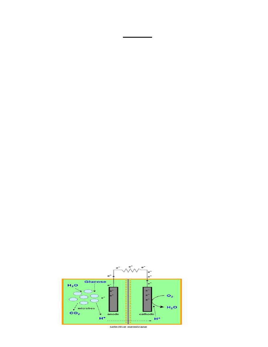
5-1-1 Carbon nanotubes - Microbial fuel cell .

Fig. 6-1 Schematic representation of microbial fuel cell
Microbial fuel cell is a device in which bacteria consume water-
soluble waste such as sugar, starch and alcohols and produces electricity
plus clean water. This technology will make it possible to generate
electricity while treating domestic or industrial wastewater.
Microbial fuel cell can turn different carbohydrates and complex
substrates present in wastewaters into a source of electricity. The efficient
electron transfer between the microorganism and the anode of the
microbial fuel cell plays a major role in the performance of the fuel cell.
The organic molecules present in the wastewater posses a certain amount
of chemical energy, which is released when converting them to simpler
molecules like CO2. The microbial fuel cell is thus a device that converts
the chemical energy present in water-soluble waste into electrical energy
by the catalytic reaction of microorganisms.Carbon nanotubes (CNTs)
have chemical stability, good mechanical properties and high surface
area, making them ideal for the design of sensors and provide very high
surface area due to its structural network. Since carbon nanotubes are also
suitable.supports for cell growth, electrodes of microbial fuel cells can be
built using of CNT.Due to three-dimensional architectures and enlarged
electrode surface area for the entry of growth medium, bacteria can grow
and proliferate and get immobilized. Multi walled CNT scaffolds could
offer self-supported structure with large surface area through
whichhydrogen producing bacteria (e.g., E. coli) can eventually grow and
proliferate. Also CNTs and MWCNTs have been reported to be
biocompatible for different eukaryotic cells. The efficient proliferation of
hydrogen producing bacteria throughout an electron conducting scaffold
of CNT can form the basis for the potential application as electrodes in
MFCs leading to efficient performance.

5-2 Catalysis.
Higher surface area available with the nanomaterial counterparts, nano-
catalysts tend to have exceptional surface activity. For example, reaction
rate at nano-aluminum can go sohigh, that it is utilized as a solid-fuel in
rocket propulsion, whereas the bulk aluminum is widely used in utensils.
Nano-aluminum becomes highly reactive and supplies the required thrust
to send off pay loads in space. Similarly, catalysts assisting or retarding
the reaction rates are dependent on the surface activity, and can very well
be utilized in manipulating the rate-controlling step.
5 -3 Phosphors for High-Definition TV.
The resolution of a television, or a monitor, depends greatly on the
size of the pixel. These pixels are essentially made of materials called
"phosphors," which glow whenstruck by a stream of electrons inside the
cathode ray tube (CRT). The resolution improves with a reduction in the
size of the pixel, or the phosphors. Nanocrystalline zinc selenide, zinc
sulfide, cadmium sulfide, and lead telluride synthesized by the sol-gel
techniques are candidates for improving the resolution of monitors. The
use of nanophosphors is envisioned to reduce the cost of these displays
so as to render highdefinition televisions (HDTVs) and personal
computers affordable to be purchase.
5 -4 Next-Generation Computer Chips.
The
microelectronics
industry
has
been
emphasizing
miniaturization, whereby the circuits, such as transistors, resistors, and
capacitors, are reduced in size. By achieving a significant reduction in
their size, the microprocessors, which contain these components,can run
much faster, thereby enabling computations at far greater speeds.
However, there are several technological impediments to these

advancements, including lack of the ultrafine precursors to manufacture
these components; poor dissipation of tremendous amount of heat
generated by these microprocessors due to faster speeds; short mean time
to failures (poor reliability), etc. Nanomaterials help the industry break
these barriers down by providing the manufacturers with nanocrystalline
starting materials, ultra-high purity materials, materials with better
thermal conductivity, and longer-lasting, durable interconnections
(connections between various components in the microprocessors).
Example: Nanowires for junctionless transistors
Transistors are made so tiny to reduce the size of sub assemblies of
electronic systems and make smaller and smaller devices, but it is
difficult to create high-quality junctions.
In particular, it is very difficult to change the doping concentration
of a material over distances shorter than about 10 nm. Researchers have
succeeded in making the junctionless transistor having nearly ideal
electrical properties. It could potentially operate faster and use less power
than any conventional transistor on the market today.
The device consists of a silicon nanowire in which current flow is
perfectly controlled by a silicon gate that is separated from the nanowire
by a thin insulating layer. The entire silicon nanowire is heavily n-doped,
making it an excellent conductor. However, the gate is p-doped and its
presence has the effect of depleting the number of electrons in the
region of the nanowire under the gate. The device also has near-ideal
electrical properties and behaves like the most perfect of transistors
without suffering from current leakage like conventional devices and
operates faster and using less energy.
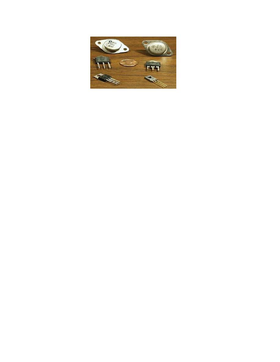
Fig.6-2 Silicon nanowires in junctionless transistors.
5-5 Elimination of Pollutants.
Nanomaterials possess extremely large grain boundaries relative to
their grain size. Hence, they are very active in terms of their chemical,
physical, and mechanical properties. Due to their enhanced chemical
activity, nanomaterials can be used as catalysts to react with such noxious
and toxic gases as carbon monoxide and nitrogen oxide in automobile
catalytic converters and power generation equipment to prevent
environmental pollution arising from burning gasoline and coal.
5-6 Sun-screen lotion.
Prolonged UV exposure causes skin-burns and cancer. Sun-screen
lotions containing nano-TiO2 provide enhanced sun protection factor
(SPF) while eliminating stickiness. The added advantage of nano skin
blocks (ZnO and TiO2) arises as they protect the skin by sitting onto it
rather than penetrating into the skin. Thus they block UV radiation
effectively for prolonged duration. Additionally, they are transparent,
thus retain natural skin color while working better than conventional skin-
lotions.

5-7 Sensors.
Sensors rely on the highly active surface to initiate a response with
minute change in the concentration of the species to be detected.
Engineered monolayers (few Angstroms thick) on the sensor surface are
exposed to the environment and the peculiar functionality
(such as change in potential as the CO/anthrax level is detected) is
utilized in sensing.